
Google's TPU Supply Chain Playbook: The Underestimated Threat to Nvidia’s AI Dominance
Investors track AMD, Amazon, and Microsoft as Nvidia’s rivals—but the most mispriced threat could be Google’s TPUs.

When the debate turns to “Who can dent Nvidia’s lead?” the same names roll off every tongue: AMD’s Instinct, Amazon’s Trainium, Microsoft’s homegrown silicon or the newer Specialized Hardware Manufacturers. Google rarely makes the list—because most assume TPUs are just an internal tool, locked away inside Google’s own data centers. That assumption is outdated. For a decade, Alphabet has been building Tensor Processing Units that already train Gemini, run at production scale, and power Google’s core revenue engines—Search, Ads, YouTube, and Cloud. The real question isn’t whether Google can build competitive silicon—it’s whether it will commercialize TPUs aggressively. If it does, the balance of power in AI hardware could shift far sooner than the market expects.
Nvidia’s $4T ascent sharpened the calculus. In the last year, Google has tested external demand—quiet pilots and capacity offers with top labs and neoclouds starved of GPUs. Names like OpenAI, Apple, and Fluidstack/CoreWeave keep surfacing in industry chatter for a reason: everyone wants credible non-Nvidia supply. But here’s the real tension that matters to investors and operators: Can Google crack CUDA’s moat and ship TPUs at Nvidia class scale—hardware, tooling, and reliability—outside its own walls? That’s the battle line.
What we’ll do in this piece:
Explain why Google is likely to step out with TPUs now—and what signals to watch in its partner playbook.
Show how TPUs differ from Nvidia’s Blackwell stack (and where they’re converging): networking, scaleout, training vs. inference, power, and TCO—with clean comparison tables.
Get practical: the moves datacenter operators, investors, and colocation providers can make if Google scales up—where to place bets, how to prepare fleets, and how to price risk.
Then, we’ll open the box: break down a TPU by component, name the suppliers, and map who stands to benefit if Alphabet turns the TPU dial to “mass.”
Why Google Can’t Afford to Sit Out the Chip Wars?
Because the market just told them. Nvidia is worth $4T doing a subset of what Alphabet does—principally silicon, platform software, and a partner cloud footprint—while Alphabet already operates the full stack: chips, compilers, global data centers, and revenuecritical AI products at planetary scale. The surprise isn’t why Google would sell TPUs; it’s why they wouldn’t unlock that value.
Because the hardware is converging. Google’s latest TPUs (v6/v7) and Nvidia’s Blackwell land on the same endgame: chiplet MCMs + massive HBM + lowprecision math (FP8/FP4) + dedicated sparsity + highradix fabrics. When physics pushes everyone to similar building blocks, the battleground shifts to scaleout efficiency, availability, and cost per token. That’s Google’s home field: multi-pod TPU meshes, optical switching, tightly engineered power/cooling, and inference first silicon tuned for price/performance at fleet scale.
Because the timing is perfect. GPUs are supplyconstrained and pricey, while inference spend is set to surpass training. Externalizing TPUs does three things at once: cuts Google’s own COGS, offers customers a credible second source beside Nvidia, and starts eroding the CUDA lockin via PyTorchXLA and JAX. If Google can match reliability and developer ergonomics outside its walls, even a single digit share of today’s Nvidia sized pie is a multi- billion dollar business—with strategic leverage far beyond mere chip sales.
Google’s Masterplan: Scaled Hardware and Software Readiness
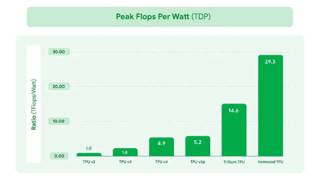
Google isn’t diving in unprepared – it’s been methodically scaling up its hardware and software for this moment. On the hardware side, Google is now on its 6th generation TPU (code-named “Trillium”) and about to launch the 7th (“Ironwood”). Each generation has dramatically increased performance and scale. Google made its TPU v6 pods widely available on Google Cloud in late 2024, and demand was immediately high. These TPU v6 chips can be arrayed into “supercomputer” pods delivering up to 42.5 exaFLOPs of aggregate compute – an astronomical figure – thanks to Google’s advanced interconnects and clustering technology. In practical terms, a TPU pod can link up to 9,216 TPU chips into one tightly-synced machine. This far outscales what’s practical with most GPU setups (even Nvidia’s largest DGX SuperPods top out at a few hundred GPUs in tight coherence). Google also outfitted its TPUs with enormous high-bandwidth memory: for example, the upcoming TPU v7 “Ironwood” will have 192 GB of HBM memory on each chip – compared to 80 GB on Nvidia’s flagship H100 GPU. That memory, running at over 7 TB/s bandwidth per chip, lets TPUs handle gigantic models and datasets smoothly. Google even developed optical switching networks to connect TPUs, slashing communication power costs and latency at the cluster scale. In short, Google has quietly built some of the most sophisticated AI supercomputers on the planet – and is now prepping them for external customers.
Testing the Waters with Key Partners
What makes Google’s TPU push credible isn’t just specs on a slide deck — it’s the fact that real customers are now paying to use them. Over the past year, Google has quietly notched a series of external deals that validate TPUs as a viable alternative to Nvidia’s GPUs. Taken together, they show a pattern: Big Tech hedging, AI labs chasing lower inference costs, and startups eager for a non-Nvidia option.
OpenAI, the most GPU-hungry company on the planet began leasing TPU capacity through Google Cloud since mid-2025, mainly for testing. While OpenAI stressed it wasn’t abandoning Nvidia, this was still pretty important for Google: Nvidia’s largest single customer was experimenting with a competitor’s chips. The driver was simple economics. Inference serving at OpenAI costs billions annually, and TPUs offered a way to shave meaningful dollars off that bill. Reports put the deal at a scale large enough to register — though notably, Google wasn’t offering OpenAI its very top-end Ironwood pods, a sign of cautious rollout.
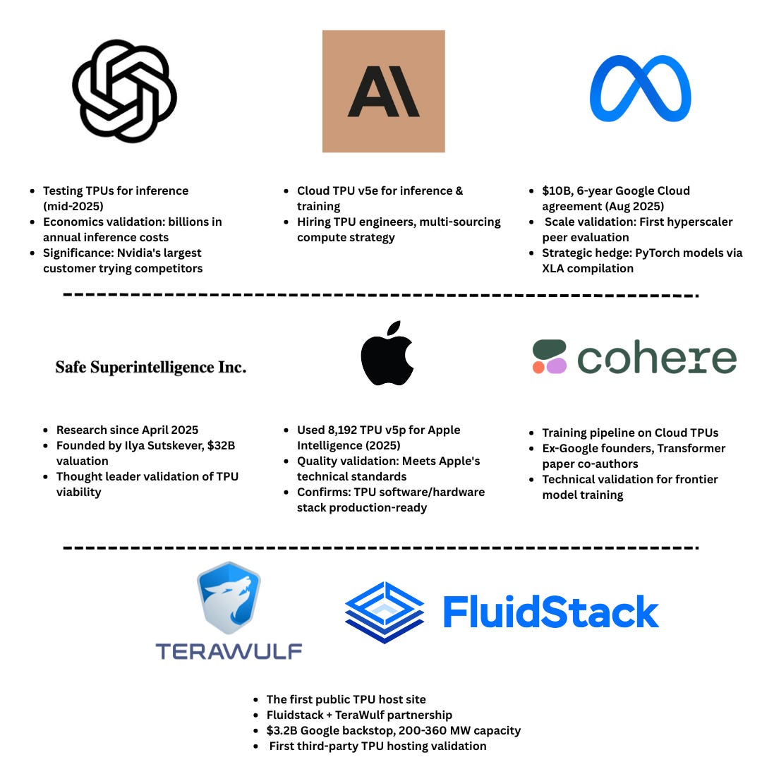
Meta is another whale. In August 2025, Meta signed a six-year, $10 billion agreement with Google Cloud to host its AI workloads. On paper, the deal is about reducing Meta’s capital expenditures — renting capacity instead of building it all in-house. But strategically, it’s hard to imagine Meta not at least evaluating TPUs within that environment. Meta’s open-source LLaMA models run on PyTorch, which now compiles to TPUs via XLA. If even a slice of that deal migrates to TPUs, it would mark the first time a hyperscaler-scale peer adopted Google’s silicon. Even if Meta ends up sticking to Nvidia GPUs inside Google Cloud, Google wins either way: it gets the revenue, and it has the chance to keep pitching TPUs.
Apple sits in a different category. It designs world‑class device chips, but trains server LLMs in the cloud. Apple’s own 2025 technical report confirms it trained Apple Intelligence server models on Cloud TPU clusters—e.g., 8,192 v5p chips—a strong signal that Google’s software/hardware stack now meets Apple’s bar. Apple won’t trumpet reliance on a rival cloud, but the fact it used TPUs speaks for itself.
Anthropic is another marquee name validating TPUs. In November 2023, Anthropic and Google said Anthropic would deploy Cloud TPU v5e at scale, initially for inference, while also highlighting training economics and MultiSlice (multi‑pod) scaling for larger model training. Google continued to feature Anthropic as a flagship Cloud customer in 2025. In parallel, Anthropic has been hiring TPU Kernel Engineers—a clear signal that it intends to keep optimizing on TPUs. Independent analysis shows Anthropic is multi‑sourcing compute: even as it expands on AWS Trainium, it’s not giving up on TPUs or Nvidia GPUs, balancing cost, availability, and performance as demand spikes.
Among startups, Safe Superintelligence (SSI) is the most strategically important. Co-founded by Ilya Sutskever — the OpenAI co-founder and chief scientist who once famously pressed Jensen Huang to sell GPUs for training AI models when they were still thought of as “gaming cards” — SSI has been using Google’s TPUs for its research since April 2025. In its most recent round, SSI raised $2 billion at a $32 billion valuation, making it one of the most highly valued AI startups pre-product. That combination matters: Sutskever has a track record of spotting hardware inflection points early, and his decision to bet on TPUs despite the glut of available capital is a signal in itself. If one of the most influential figures in AI is willing to tie his new lab’s compute destiny to Google’s chips, investors and operators should pay attention.
Cohere, the Canadian LLM company behind the Command family of models, has also been building on TPUs. The choice isn’t accidental — several ex-Googlers sit in its technical leadership, including co-founder Aidan Gomez, who co-authored the original “Attention Is All You Need” Transformer paper while at Google Brain. Cohere has already moved part of its training pipeline onto Google Cloud TPUs, citing cost and throughput gains as models scale. And for Cohere, it’s a hedge — access to high-end compute without competing head-to-head for scarce Nvidia GPUs. While the immediate dollar value may only be in the tens of millions, the significance lies in Cohere’s stature as a top-tier LLM lab: its use of TPUs validates the hardware as production-grade for frontier-model training, not just inference experiments.
Google has also seeded TPUs deeply into academia, getting students familiar with its ecosystem. Through the TPU Research Cloud (TRC), thousands of researchers have received free access to pods of Cloud TPUs, enabling open-source milestones like EleutherAI’s GPT-J (6B) training run on a v3-256 pod. TRC spotlights show mainstream PyTorch projects, such as the timm vision library, relying on TPUs—proof that PyTorch-XLA is production-ready outside Google. At the entry level, Colab and Kaggle TPUs let students prototype on the same accelerators that power Google’s data centers, creating habits that follow them into startups and labs. And with Google’s $1 billion university initiative announced in 2025, offering cloud credits and advanced tooling, TPU literacy is being institutionalized at scale. Strategically, this academic pipeline matters: CUDA became dominant because a generation of researchers learned it by default; Google is now trying to ensure the next wave of AI talent grows up just as comfortable with JAX and PyTorch-on-TPU, creating latent demand that will spill into industry.
On the Neocloud Front : Fluidstack + TeraWulf: the first public TPU host site
The clearest signal that Google will place TPUs outside its own campuses came mid August 2025 when TeraWulf announced it would host 200 MW (expandable to 360 MW) for Fluidstack at Lake Mariner (NY), backed by Google’s $1.8B financial backstop and warrants equal to ~8% proforma equity. On Aug 18, TeraWulf disclosed Google increased the backstop to ~$3.2B and its stake to ~14% via additional warrants.
How the structure works. The TPUs will be physically deployed at TeraWulf’s Lake Mariner site, operated by Fluidstack, which leases the power and space. Google acts as (1) anchor backer—guaranteeing financing against Fluidstack’s longterm leases—and (2) strategic investor—taking equity exposure to the site operator (TeraWulf). This lets Google place TPUs in a thirdparty colo without owning the real estate, while still controlling access to the chips. Google has also reportedly approached CoreWeave and Crusoe.
Essentially Google is using selective partnerships to validate TPUs in the wild — inference at OpenAI, AI research at Apple and SSI, training at Cohere, hosting at Fluidstack, large-scale capacity at Meta. Each deal acts as a real-world stress test of both hardware and software. Every bug fixed for OpenAI’s ChatGPT pipeline, every PyTorch operator patched for Cohere, every data-center reliability issue surfaced by Fluidstack — it all strengthens the TPU offering.
That’s why the rollout looks slow and cautious: it’s not just about renting compute; it’s about hardening the ecosystem. By the time Google scales TPU access broadly, it will have the credibility of saying: these chips already run workloads from OpenAI, Apple, Meta, Cohere, and SSI. That kind of validation will be necessary for Google to prove credibility.
From Neo-Cloud Distress to Google’s Advantage
Neoclouds thrived when GPUs were scarce, but scarcity isn’t a business model. Many financed growth at high rates, signed longterm power leases, and sold shortterm contracts at markups that only made sense in a crisis. Now, as Nvidia ramps supply and hyperscalers build aggressively, those same commitments are turning into liabilities.
For Google, this dislocation is an entry point. Unlike GPU only operators, it controls the silicon and the software; unlike traditional REITs, it has the balance sheet to underwrite power. By stepping into stressed structures—through lease guarantees (as with Fluidstack/TeraWulf), warrants in site operators, or utilization floors that derisk financing—Google can expand TPU footprint at a discount. For landlords, a TPU pod underwritten by Google lowers cost of capital and reopens financing channels. For Google, it’s a way to grow globally without pouring billions into its own concrete.
Even private capital that typically shows up only in distressed cycles is paying attention. If TPU deployments reunderwrite stranded megawatts into financeable infrastructure, the pool of partners isn’t limited to operators alone. Recent multiyear, multibillion AIinfra contracts (e.g., Microsoft–Nebius) illustrate how anchor deals can rerate digital assets and reopen capital markets.
Crucially in the paid section later in this report we will explore how Google, neo-clouds, and datacenter operators might jointly win by aligning around TPU deployments, but first its worth exploring how TPUs actually stack up against the incumbents. Benchmarks and software support are where reputations are made or broken. To understand Google’s chances of breaking into a CUDA-dominated market, we need to compare TPU performance and developer tooling head-to-head with Nvidia’s Blackwell GPUs and AMD’s Instinct line.
TPU Architecture and the Convergence with Blackwell
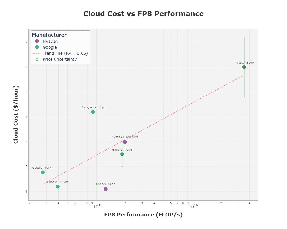
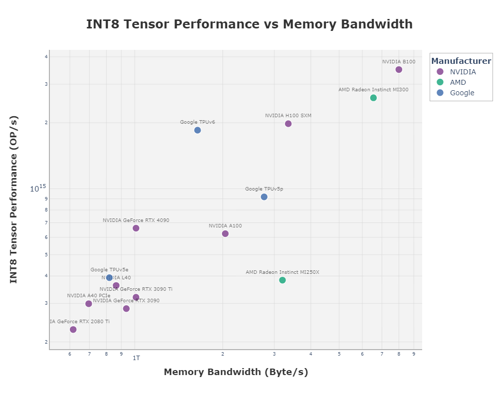
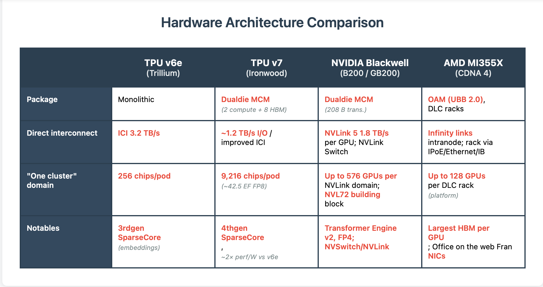
Google’s latest TPUs and NVIDIA’s newest GPUs have converged on a surprisingly similar physics‑driven design philosophy. Both have abandoned the idea of a giant monolithic die in favor of chiplet packaging, surrounding compute cores with vast stacks of high-bandwidth memory.
With TPU v7 “Ironwood,” Google packages two compute dies plus eight HBM stacks (≈192 GB total, ~7.2–7.4 TB/s); Google quotes ~4.6 PFLOPS FP8 per chip and pods of 256 or 9,216 chips. The Register pegs per‑chip power in the ~700 W–1 kW class.
NVIDIA Blackwell (B200/GB200) follows a similar dual‑die design (≈208 B transistors on TSMC 4NP) and pushes FP8/FP4 math via Transformer Engine v2. NVIDIA markets NVL72 as a single 72‑GPU NVLink domain; NVLink Switch can extend that fabric up to 576 GPUs before you step out to InfiniBand/Ethernet. NVIDIA continues to publish the most concrete system numbers (e.g., DGX B200: 72 PFLOPS training FP8; 144 PFLOPS inference FP4 for 8 GPUs).
The physics of modern AI left both companies with no choice but to build toward the same frontier.
Where the divergence shows is in scale. NVIDIA’s NVLink interconnect tops out at around seventy-two GPUs in a tightly coupled configuration before handing off to InfiniBand or Ethernet, which adds latency and complexity. Google built its TPU pods to scale to thousands of chips natively, with a custom interconnect and optical switching fabric. The result is that Google can train trillion-parameter models across nine thousand TPUs in a single pod with relatively little overhead. For workloads that truly need that level of synchronization, TPU remains the cleaner path.
Failed to render LaTeX expression — no expression found
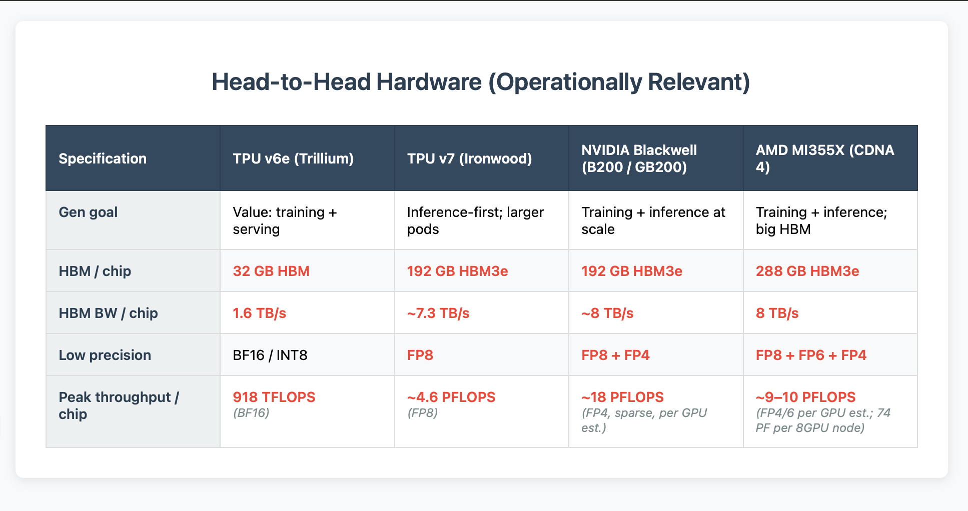
Sources: TPU v6e spec table (HBM/BW/ICI/TFLOPs).
Ironwood memory/BW/FP8 perchip, 256/9,216chip pods, 2× perf/W claims.
Blackwell MCM + NVLink5 + NVL72 domain.
AMD MI350/MI355 memory/BW/FP6/FP4; platform scaling
Software, Ecosystem, and the CUDA Moat (drop in replacement)
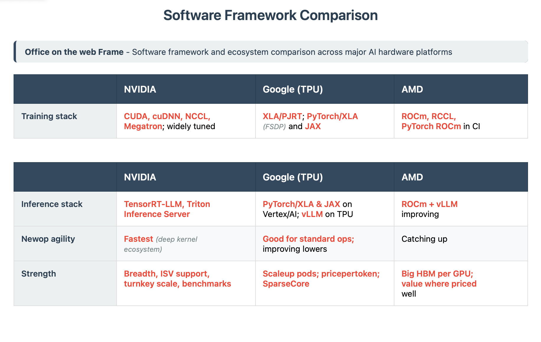
Hardware doesn’t win adoption—developer experience does. NVIDIA still sets the pace with CUDA + cuDNN + NCCL for training and TensorRTLLM + Triton Inference Server for serving, which makes “runs on day one” the default for most teams. Google has closed much of the practical gap for mainstream LLM/RAG/recsys: PyTorch on TPU via OpenXLA/PJRT (PyTorch/XLA), JAX for research, vLLM on TPU for highthroughput inference, and widespread access through the TPU Research Cloud. AMD’s ROCm has improved (PyTorch CI, broader kernels), but it’s still less turnkey than CUDA or Google’s current TPU toolchain. Net: NVIDIA remains the broadest, lowestfriction path; Google is now a credible choice when efficiency/scale drive the decision; AMD is catching up, with momentum but a usability delta. AMD does work really great for smaller workloads now however and has a TCO and performance edge for certain models over NVIDIA.
Note: NVIDIA Triton Inference Server (for deployment) is different from OpenAI Triton (a kernel DSL); the name collision confuses newcomers.
Who Wins Where: Training, Inference, Model Shifts, and the Edge
Training at frontier scale. In practice, there are two proven paths today for finished frontierscale pretraining runs: NVIDIA Hopperclass clusters (H100/H200) and Google TPUs. Meta’s Llama 3.1 405B and similar large releases have been trained on NVIDIA’s platform, while Google’s Gemini 2.5 family is trained on TPUs. NVIDIA’s newest Blackwell parts (B200/GB200) are ramping, with strong results in MLPerf Training and major inference milestones, but we haven’t seen a tier-one lab publicly release a flagship model trained end-to-end on Blackwell yet. Expect that to change as NVL72 deployments spread.
Why TPUs remain credible for the very largest jobs.
Google designed pods as native scaleup machines: Ironwood (TPU v7) composes 256 chip and 9,216 chip pods with an optical fabric and ICI links, yielding ≈42.5 EF FP8 and ≈1.77 PB of shared HBM in one tightly synchronized domain. That system design keeps collectiveop overhead unusually low for trillionparameter training. NVIDIA’s NVL72 is a 72GPU NVLink domain per rack; NVLink Switch can extend further (NVIDIA cites fabric scales up to 576 GPUs) but most realworld builds step out to InfiniBand/Ethernet beyond that boundary. Translation: TPUs still offer the cleanest single system image at extreme node counts, while NVIDIA dominates breadth and availability.
Inference at scale.
Two stories are unfolding. First, Google’s Ironwood is inference-first silicon: FP8 throughput, 192 GB HBM3e per chip, and Google reported ~2× perf/W vs Trillium. It exists to cut cost per million tokens in cloud serving while keeping long contexts resident. Second, NVIDIA keeps setting public tokens per second records with Blackwell software stacks (TensorRTLLM, Transformer Engine), which matters for low latency, high throughput serving. In other words, TPUs press the TCO angle; NVIDIA presses timetoresult and ecosystem.
Model architecture shifts (who adapts fastest).
When researchers add a new attention variant or operator, the winner is whoever gets kernels and graph compilers updated first and broadly. That’s still NVIDIA: CUDA + cuDNN + NCCL + TensorRT/Triton and a decade of kernel IP make “dayone” support likely. Google has closed much of the gap for mainstream ops through PyTorch/XLA (PJRT) and JAX, and the pace is visible in recent PyTorch/XLA releases (including vLLM support). AMD’s ROCm is improving (PyTorch CI, ROCm 7), but remains less turnkey for novel ops. Net: if you are betting on rapid model innovation, NVIDIA minimizes integration risk; if your workload is standard LLM/RAG/recsys and you care most about cost/token, TPU is credible; AMD is viable where its memory profile fits, with diligence on software.
Memory-bound single device work.
If your bottleneck is “fit it all on one device” (huge embeddings, very long context windows, large MoE experts), AMD’s MI355X is the capacity leader at 288 GB HBM3e and 8 TB/s per GPU, with rack level disclosures up to 128 GPUs using Pollara NICs. This can simplify sharding and improve tail latency—provided the kernels you need are mature on ROCm.
What about AWS Trainium, Tesla, and Meta’s chips?
AWS Trainium 2 is scaling (Rainier-class superclusters; Anthropic names AWS its primary training partner) but lacks a publicly finished frontier model so far; Tesla/XAI are focusing its own silicon on inference the AI5 and AI6 chips while leaning on heavily on NVIDIA GPUs for training in their data centers; Meta MTIA is live for recommendation inference and testing a training part, with NVIDIA still carrying Llama-class training. At the edge, NVIDIA Jetson → AGX Thor dominates performance robotics, Apple’s Neural Engine anchors on device consumer AI, and Google Edge TPU plays targeted roles .Edge and “physical AI.” The center of gravity at the edge is NVIDIA Jetson, now evolving from Orin to Jetson AGX Thor (Blackwellbased), with early adopters across robotics and industrials. On devices, Apple’s Neural Engine powers ondevice Apple Intelligence models, with server models handling heavier requests
Performance robotics (mobile manipulators, AMRs, humanoids) overwhelmingly standardizes on NVIDIA Jetson today and Jetson AGX Thor next because it brings the same CUDA/Isaac stack as the datacenter into 30–100 W modules, handles multisensor fusion and realtime control, and now adds Blackwellclass transformer throughput for visionlanguage policies. Consumer ondevice AI is led by Apple’s Neural Engine on A/Mseries chips (private, lowlatency experiences like Apple Intelligence), with Qualcomm and MediaTek NPUs saturating Android phones and new Copilot+ PCs—huge in volume even when singledevice models are modest. The third segment—industrial/IoT edge (cameras, gateways, retail/telemetry)—leans on Google’s Edge TPU/Coral and similar lowpower ASICs for alwayson, quantized inference where watts and BOM dominate; they’re superb at sustained detection/classification but not meant for longcontext LLMs. Read this as segmentation, not competition: Jetson/Thor wins where realtime performance and CUDA compatibility matter; Apple/phone/PC NPUs win ubiquitous, privacypreserving experiences; and Edge TPUclass parts win costandpowerconstrained deployments. Together they expand the total edge TAM—and they also pull cloud demand (training and fleet scale orchestration), which is why the datacenter race and the edge race are tightly coupled.
Looking Ahead
Chiplets, HBM and lowprecision math are locked in; the real separation will be scale, software, and unit economics.
In the next few years Inference will overtake training as the spending center, and buyers normalize on cost per million tokens at a latency SLA. If google plays their cards right TPUs should become the credible second source: expect at least one marquee external win where Ironwood pods beat comparable GPU fleets on cost per token while meeting SLOs. NVIDIA should still own the “dayone” path—its ecosystem ships new kernels fastest—and even if share redistributes, a bigger pie plus Blackwell ramp keeps revenue growing. AMD is well on its way to fixing the memory and networking shortcomings and should capture memorybound niches (288 GB HBM per GPU) as context windows expand—provided ROCm is locked down for those workloads. Specialist silicon settles into home turf: Trainium2 for inAWS cost/control, MTIA for recsys (training to follow), Tesla AI5/AI6 for lowlatency autonomy/robotics. Cerebras, Groq and Samanova are also worth keeping an eye on.
The edge splits three ways—Jetson/Thor for performance robotics, phone/PC NPUs for private ondevice AI, lowpower ASICs (EdgeTPU class) for industrial/IoT—and each pulls more cloud training and orchestration. New KPIs—tokens/joule, tokens/rack, cost per million tokens @ P95—replace FLOPs in procurement. And because networks and cooling decide who can keep collectives tight at scale, opticalheavy fabrics and liquid cooling become kingmakers. Bottom line: this is a portfolio market—NVIDIA remains the broad onramp, Google wins scale up and cost per token, AMD wins per device memory—so everyone can grow even as share shifts.
Meanwhile, Nvidia isn’t complacent – it will likely respond by offering more integrated solutions (e.g., Nvidia may bundle software and even cloud-like offerings via partners, as it’s doing with DGX Cloud). It’s also possible Nvidia might cut prices or offer leasing models if it feels pressure. But Nvidia also has to be careful not to undermine its own massive margins. Google, in contrast, could even treat TPU offerings as a loss leader to grow cloud market share (since Google’s overall business benefits if you come to its cloud).
In the end, the AI hardware race is entering a new phase. For years it was all about GPU vs GPU (Nvidia vs AMD vs Intel’s fledgling attempts). Now it’s shifting to GPU vs specialized accelerators vs hyperscaler-designed chips. Google’s entry instantly makes the fight more interesting. And unlike a startup, Google has deep pockets to fund this and a huge internal use-case guaranteeing that TPUs won’t go unused.
In the free section above, we explored Google’s motivations, technology and strategy in taking on Nvidia, and how TPUs compare to the current and next-gen GPUs.
In the subscribers-only section to follow, we will delve into the often-overlooked side of this equation:
1) The TPU Anchor Structures — For neoclouds looking to expand, or under pressure and financiers looking for stability, this section lays out clear deal templates to de-risk growth. Think anchor agreements, guaranteed offtakes and the ability to land long term deals that align smaller players with larger operators and spread risk beyond a single supplier. The playbook shows how fragile, spot-based GPU income can be converted into steady TPU-backed cashflows—contracts that lenders and investors can actually underwrite.
2) The TPU Supply Chain Winners — In this deep dive, we map the companies (public and private) that stand to gain if Google meaningfully scales TPU production—and the broader set of suppliers riding the AI accelerator wave across all hyperscalers. From fabs and HBM vendors to substrate makers, optics providers, and liquid-cooling OEMs, we’ll show you who is already winning orders, where bottlenecks lie, and which sectors are best positioned for durable growth. For investors, this is a forward-looking tracker of the stocks and categories most levered to TPU and GPU demand. For neoclouds and operators, it’s a practical view of which partners are emerging as critical—and how to align site specs to capture anchor status.