
Part 2 : Beyond Power : The Networking Bottleneck Starting to take Shape
Copper, optics, and where the real bottlenecks and value pools are

If you watch the AI hype cycle, it looks like GPUs and TPUs are doing all the work. In reality, they’re just the muscles. The nervous system that makes an AI factory useful is the network: a stack of copper traces, cables, fibers, and optics that moves bits from chip to chip, rack to rack, datacenter to datacenter, and eventually out to users.
That network is no sideshow. Data‑center Ethernet switching is already a low‑$20B annual market, with forecasts showing it rising toward the mid‑$30Bs by 2028 as hyperscalers expand AI back‑end and front‑end fabrics, growing high‑single digits annually, while the optical transceiver market is already in the low‑teens billions with mid‑teens CAGR, driven heavily by AI datacenter upgrades. Analysts expect shipments of 400G/800G datacom optical modules to climb from about $9 billion in 2024 toward $16 billion by 2026, with 800G modules and soon 1.6T driving the next wave. That’s before you count the backbone optics that tie regions and continents together.
So this isn’t just a “supporting cast.” It’s a fast‑growing capital line item and a potential bottleneck for every large‑scale AI deployment.
FPX Services: This report details the critical bottlenecks in AI scaling. If you are an investor or operator looking to navigate these supply chains, model TCO, or secure hardware capacity, FPX provides the execution layer to turn these insights into action. Explore our consulting services here.As always this is Not investment advice; for informational purposes only. The clearest way to understand it is to follow a single bit as it travels:
From one GPU/TPU to another inside a server
Across servers inside a rack
Across racks inside a datacenter (leaf–spine)
Between buildings on a campus
Between datacenters across a metro (DCI)
Across metro, long‑haul, and subsea fiber back to other regions and, ultimately, users
At every step you can ask three questions:
Is this electrons in copper, or photons in glass?
Which components and materials are in play?
Who in the value chain actually makes money here?
Let’s go ring by ring.
Paid Subscribers get a TL;DR version at the end of the report if you only want the key takeaways.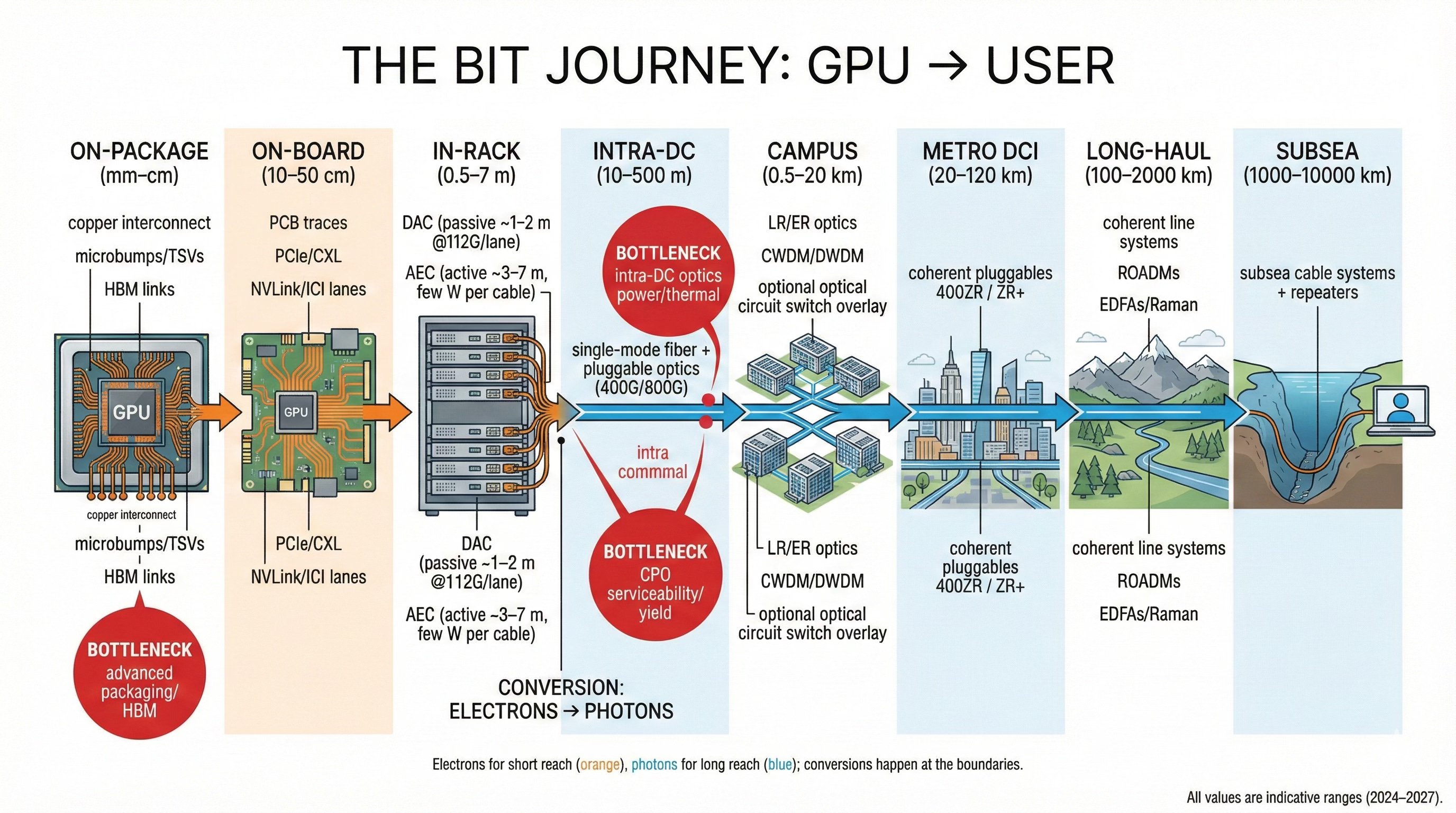
1. Inside the server: why everything is copper at short range
Start with something concrete: a rack‑scale AI system like Nvidia’s GB300 NVL72, which ties 72 Blackwell Ultra GPUs and 36 Grace CPUs into a single liquid‑cooled rack. Inside that rack, each GPU exposes 18 NVLink 5 connections running at 100 GB/s each, for 1.8 TB/s of bidirectional bandwidth per GPU and 130 TB/s of NVLink bandwidth across the system. Google’s TPU v5p pods wire together 8,960 chips with 4.8 Tb/s of inter‑chip interconnect (ICI) per chip in a 3D torus; the newer Ironwood (TPU v7) superpods scale to 9,216 chips with 9.6 Tb/s per chip of ICI and ~1.77 PB of HBM3E addressable memory.
All of that is happening over copper.
Inside a package, between GPU compute dies and stacks of HBM, the information moves through microscopic copper interconnects in silicon and package substrates. You have:
Thin copper traces in the chip’s metal layers
Through‑silicon vias (TSVs) and microbumps connecting dies to HBM
Organic substrates or silicon interposers that fan signals out to the package edge
Once you leave the package, you land on a PCB (printed circuit board): a sandwich of fiberglass/epoxy and copper that routes signals between GPUs, CPUs, NICs, and switch ASICs. At this point, everything is still just a voltage pattern on a copper trace.
The key enabling block here is the SerDes (serializer/deserializer) built into every high‑speed chip. A GPU doesn’t push a 1.8 TB/s firehose on a single wire; it spreads that bandwidth across many high‑speed serial lanes. NVLink 5, for example, runs at 100 gigabytes per second per link, and each Blackwell GPU supports 18 such links to reach 1.8 TB/s. Those lanes are amplified, equalized, and shaped to survive a few centimeters of PCB and maybe a connector or two.
Why is everything copper here?
Because at centimeter‑scale, copper is unbeatable on cost, latency, and simplicity. The signal hasn’t had time to attenuate much; you can route dense, multi‑terabit connections with nothing more exotic than carefully designed copper traces and connectors. Lasers would make this more complex, not less. The bottleneck becomes SerDes design and signal integrity engineering, not the medium.
From an investor’s perspective, this short‑reach domain belongs to:
GPU/TPU and CPU vendors, who control the SerDes and package design
Switch/NIC/DPU vendors, who expose hundreds of SerDes lanes per chip
A handful of PCB and substrate suppliers that can handle the signal‑integrity demands of 112–224 Gb/s per lane
None of this looks like “optics,” but it directly drives demand for optics: the more high‑speed lanes a GPU or switch exposes, the more off‑rack bandwidth you need to move data out of that system.
What Companies are working in this space
Inside this “all-copper” domain, a relatively small set of companies quietly control most of the value chain. At the top sit the compute vendors – NVIDIA (NVDA), AMD (AMD) and the hyperscaler silicon teams inside Alphabet (GOOGL), Amazon (AMZN) and Microsoft (MSFT) – who decide how many SerDes lanes exist, at what speeds, and with which protocols (NVLink, Infinity Fabric, PCIe, CXL, TPU ICI, etc.). Every extra lane and every bump in per-lane speed multiplies pressure downstream: more I/O pins, more substrate layers, more PCB complexity, more connectors, more signal-conditioning silicon. Right next to them in the stack are the HBM memory suppliers – SK hynix (000660.KS), Samsung Electronics (005930.KS), and Micron (MU) – whose stacked DRAM sits on the same package and effectively defines how wide and how hot that on-package copper fabric must be; HBM capacity and yields are now as constraining to AI throughput as the GPU dies themselves.
Underneath that, you have the “infrastructure of copper” that makes these short-reach electrons possible. Advanced packaging and assembly are handled by foundry/OSAT players like TSMC (TSM), Intel (INTC), ASE Technology (ASX) and Amkor (AMKR), which turn bare dies plus HBM stacks into huge 2.5D packages and must supply enough CoWoS-class capacity to keep GPU releases on schedule. Those packages sit on IC substrates built with Ajinomoto (2802.T)’s ABF film (essentially a near-monopoly insulator for high-end substrates) and manufactured by houses like Ibiden (4062.T), Shinko (6967.T), Unimicron (3037.TW) and AT&S (ATS.VI). From there, server and accelerator PCBs come from fabricators such as TTM Technologies (TTMI) and Unimicron, populated with high-speed connectors and internal copper assemblies from TE Connectivity (TEL), Amphenol (APH) and Molex (private), and stitched together electrically by retimer/clocking and SerDes-adjacent silicon from Broadcom (AVGO), Marvell (MRVL), Credo (CRDO), Astera Labs (ALAB), Analog Devices (ADI) and Texas Instruments (TXN). None of these companies sell “optics,” but collectively they define how far you can push electrons on a board or inside a chassis, how many lanes you can route, and how much power/latency that costs. In other words: the more bandwidth you squeeze out of this copper stack, the more inevitable it becomes that the next hop – off the board and out of the rack – must be solved with fiber and optics.
2. Inside the rack: harnesses, DACs, and active copper
Now zoom out a bit. A rack like the NVL72 or a TPU superpod chassis is basically a small city of copper.
Within that rack:
GPUs connect to each other and to NVSwitch or similar fabrics over short copper links.
Servers or trays connect to the top‑of‑rack (ToR) switch using copper cables up to a few meters long.
In TPU pods, chips inside a cube or block are wired over PCB and internal copper harnesses before traffic is ever turned into light.
At this distance scale—roughly 0.5–7 meters—the industry splits copper into two regimes:
Passive DAC (Direct Attach Copper).
For very short runs (0–2 or 3 m), you can get away with simple twinax copper cables with no active electronics in the ends. The SerDes in the GPU or NIC pushes a PAM4 signal directly down the wire, and the receiver reconstructs it. This is the cheapest, lowest‑latency option.
Active Electrical Cables (AEC/LACC).
Once you push toward 3–7 m at 100–200 Gb/s per lane, copper behaves like a severe low‑pass filter—loss and reflections shred your eye diagram. To stay with copper instead of jumping to optics, vendors embed DSPs or linear amplifiers in the cable ends. Those chips equalize and reshape the signal so it can survive longer runs. Companies like Credo built their entire business around these Active Electrical Cables, and you saw them show up early in large AI systems such as Intel’s Gaudi platforms and early GPU clusters.
You can think of AECs as a bridge technology: they buy hyperscalers a few more meters of copper at each speed node so they don’t have to flood racks with optics too early. The value is extremely tangible: a rack full of AOCs (active optical cables) can burn almost as much power as the switches they connect; a rack using AECs and short DACs buys back real watts without sacrificing speed.
From a materials perspective, you’re still dealing with:
Copper twinax cables
High‑frequency connectors
Small DSP/retimer chips in the cable ends
All of these live in a brutally cost‑sensitive environment. But as line rates climb (112 → 224 Gb/s per lane), the willingness to pay for smarter copper increases. That’s why AEC and PAM4 PHY vendors are so leveraged to AI networking: they sit exactly where “just run more DACs” stops working.
What Companies are working in this space
At this distance scale you can also start to see a very clear stack of specialized vendors. At the physical layer, connector and cable OEMs like TE Connectivity (TEL), Amphenol (APH), Molex (private), Luxshare Precision (002475.SZ) and Foxconn Interconnect Technology (6088.HK) manufacture the twinax assemblies, high-speed connectors, and internal harnesses that physically bind GPUs, switches, and trays together. Their job is brutally practical: hit tight insertion-loss, crosstalk, and thermal constraints at the lowest possible cost per port, while scaling to millions of identical links. Because hyperscalers want predictable impedance and easy field replacement, these vendors effectively industrialize “copper as a modular building block” inside every rack.
Layered on top of that are the silicon players that turn dumb copper into active copper. Credo (CRDO), Marvell (MRVL) and Broadcom (AVGO) ship the PAM4 DSPs and retimer PHYs that live in the ends of AECs and high-speed copper links; they’re the reason a 224 Gb/s lane can survive several meters of lossy twinax instead of dying after a meter or two. System OEMs like NVIDIA (NVDA), Cisco (CSCO), Arista (ANET) and Juniper (JNPR) then qualify and brand end-to-end cable SKUs for their GPU and switch platforms, deciding where to use cheap passive DACs, where to pay up for AECs, and where to flip to optics. In other words, the economics of “how far can we push copper before we’re forced into fiber” flow through this whole chain—cable OEMs monetize volume, DSP vendors monetize every extra dB of reach, and the system vendors arbitrage the mix to minimize watts and dollars per terabit inside the rack.
3. Inside the datacenter: leaf–spine over fiber
Take one more step back. Inside a modern AI datacenter, racks don’t talk to each other directly; they talk through a fabric of switches—typically some form of Clos/leaf–spine topology.
At the bottom tier, you have a ToR or leaf switch in each rack. Above that, multiple spine switches connect every leaf. Any rack can reach any other in two hops: leaf → spine → leaf. For very large sites, a third super‑spine layer ties clusters of spines together.
Logically, this gives you:
Predictable latency
High bisection bandwidth
A structured place to scale from one AI cluster to many
Physically, it forces you off copper and onto fiber.
Inside the row, and certainly between rows, you’re usually looking at 10–500 meters of reach. At 400G and especially 800G per port, copper is simply not economical at those distances—the power you’d spend on equalization and retimers would be insane. So racks connect up to leaf/spine switches using optical transceivers and fiber.
In 2024–2025, mainstream hyperscale fabrics are largely:
400G ports built from 4×100G PAM4 lanes
800G ports built from 8×100G or 4×200G PAM4 lanes
Transitioning toward 1.6 Tb/s ports on next‑gen switch silicon and optics roadmaps
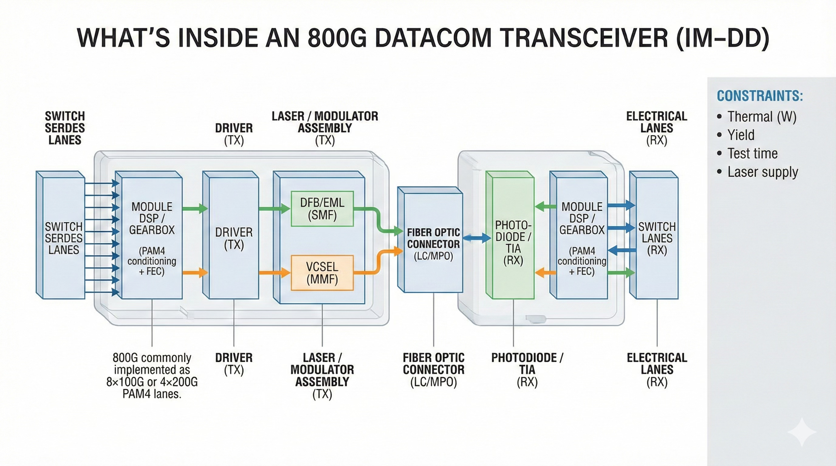
Those ports are exposed through pluggable modules (QSFP‑DD or OSFP) that contain:
A PAM4 DSP
One or more lasers (DFB/EML for single‑mode, VCSEL for multimode)
Modulators, photodiodes, TIAs
A fiber connector (often MPO or LC)
For distances within a building, most hyperscalers standardize on single‑mode fiber (SMF) and IM‑DD optics:
DR / DR4 for ~500 m single‑mode
FR / FR4 for ~2 km single‑mode
Multimode SR is still used in some environments, but the shift to SMF is well underway because it simplifies plant and supports higher speeds over longer runs.
Under the hood, switch ASICs are now in the 100 Tb/s class. Broadcom’s Tomahawk 5 and 6 families, for example, offer up to 102.4 Tb/s per chip—enough for 128×800G ports or similar combinations—while Nvidia’s Quantum‑X InfiniBand and Spectrum‑X Ethernet switches deliver hundreds of 800G ports for AI fabrics.
All of this is still powered by SerDes, but now the copper is very short: a few centimeters from the switch ASIC to the optical module. Nearly all of the distance is carried in glass.
This is where the optics market really scales: millions of 400/800G modules per year, low‑teens‑billion‑dollar revenue globally and growing mid‑teens annually, with AI clusters as a key demand driver for early adoption of 800G and 1.6T.
What Companies are working in this space
Inside this leaf–spine layer, what you’re really looking at is a small group of companies that decide how “AI bandwidth” is packaged and sold. On the system side, Arista Networks (ANET) and NVIDIA (NVDA) are effectively the dual keystones of high-performance fabrics: Arista dominates “pure Ethernet” at the top end, selling stateless Clos building blocks plus EOS and automation that let hyperscalers stitch 100+ Tb/s ASICs into predictable fabrics; NVIDIA, meanwhile, owns the specialized AI fabric stack with Quantum-X InfiniBand and Spectrum-X Ethernet, bundling switches, NICs/SuperNICs, and software (SHARP offload, congestion control, collectives libraries) into a vertically integrated offering tuned for all-reduce and model-parallel traffic. Cisco (CSCO) still anchors a huge portion of the datacenter switch TAM, combining its Nexus/Silicon One platforms with a captive optics strategy (via Acacia and Luxtera) to sell end-to-end IP/optical solutions to both cloud and enterprise, and now HPE (HPE) has effectively absorbed Juniper’s (ex-JNPR) data-center routing/switching franchise, giving it a credible spine/leaf story tied into HPE’s server and storage lines. In parallel, Celestica (CLS) and Accton (2345.TW) are the ODM muscle behind many “white-box” deployments – they take merchant silicon (Broadcom, Marvell, sometimes NVIDIA), wrap it into 1U/2U pizza boxes, and ship them by the tens of thousands into AI back-end networks where brand matters less than cost, power, and time-to-rack.
From a first-principles perspective, these vendors collectively answer three questions for the operator:
(1) Who controls the forwarding behavior and failure modes of the fabric? (Arista’s EOS, NVIDIA’s Infiniband stack, Cisco/HPE NOSes.)
(2) Who integrates the switch ASIC, optics, and mechanics into something that survives at 20–30 kW per rack? (Arista/Cisco/HPE on the branded side; Celestica/Accton on the ODM side.)
(3) Who sets the price-per-terabit curve as port speeds ratchet from 400G → 800G → 1.6T? Here, ANET and NVDA effectively define the top-end “AI fabric SKU” economics, while CSCO/HPE protect share in more general DC fabrics, and CLS/Accton compress margins from below by giving hyperscalers cost-optimized white-box gear.
All of them are tightly coupled to the same underlying constraints (Broadcom/Marvell switch ASIC roadmaps, 400/800G optics availability, rack power envelopes), but their business models sit at different layers of the stack: Arista/NVIDIA/Cisco/HPE monetize software, ecosystem, and support on top of merchant or custom silicon, whereas Celestica/Accton monetize volume manufacturing and integration efficiency. As port speeds climb and optics consume a larger fraction of switch BOM, the players that can co-design fabric topology + NOS + optics strategy (ANET, NVDA, CSCO, HPE) will have disproportionate leverage over how big an AI cluster can practically get and what each incremental terabit of leaf–spine capacity costs.
4. Co‑packaged optics: shrinking the electrical domain
At 800G, and especially 1.6 Tb/s per port, even the few centimeters of PCB between switch ASIC and pluggable optics start to hurt. You can throw more DSP at it, but you pay in power and latency. Nvidia’s own internal modeling for traditional architectures shows that a 400,000‑GPU AI “factory” could burn on the order of 70+ megawatts just in optics and switching if you stick with classic pluggables.
The industry’s answer is co‑packaged optics (CPO) and silicon photonics:
Move the optical engines onto the same package as the switch ASIC.
Shorten the electrical path from centimeters of PCB to millimeters of interposer.
Lower electrical loss, which lets you cut transmit power and DSP complexity.
At GTC 2025, Nvidia announced Quantum and Spectrum switches with embedded photonics and CPO, claiming up to 1.6 Tb/s per port and more than 50% reduction in network power compared to traditional pluggable transceivers at scale. STMicroelectronics, in collaboration with AWS, has separately announced photonics chips for AI datacenter transceivers, and market researchers like LightCounting expect the optical transceiver market to grow from around $7 billion in 2024 to $24 billion by 2030, driven by these kinds of deployments.
For investors, CPO is important because it reshuffles the value chain:
More value moves from module vendors to switch/NIC vendors + photonics engine suppliers.
Packaging and silicon‑photonics process know‑how become major moats.
Power per bit—the ultimate scarce resource in AI datacenters—becomes the central selling point.
What Companies are working in this space
Co-packaged optics pulls a very different cast of characters into the center of the networking story. At the system level, NVIDIA (NVDA), Broadcom (AVGO), and Cisco (CSCO) are no longer just selling boxes with slots for other people’s modules — they are designing electro-optical machines where the switch ASIC, photonics engines, and package are co-designed as a single organism. NVIDIA’s Spectrum-X Photonics and Quantum-X Photonics families take this to its logical extreme: 1.6 Tb/s-per-port switches that integrate silicon-photonic engines on the same package, eliminating faceplate pluggables and, by NVIDIA’s own numbers, cutting network power by roughly 3.5× and boosting resiliency by an order of magnitude for “million-GPU AI factories.” Broadcom (AVGO) plays the merchant analog: its Tomahawk 6 “Davisson” 102.4 Tb/s Ethernet switch co-packages 16 × 6.4 Tb/s optical engines around the ASIC, inheriting experience from its earlier Tomahawk 5 “Bailly” 51.2 Tb/s CPO switch and using TSMC’s COUPE photonic engine to drive 64 × 1.6 TbE ports at 200 G/lane. Cisco (CSCO), for its part, has demonstrated full CPO routers using Silicon One ASICs with co-packaged silicon-photonics tiles, and publicly commits to CPO as a way to collapse SerDes count and cut per-bit power while keeping an open, multi-vendor ecosystem around optics rather than locking everything to a single in-house module line.
Underneath those system brands sits a new “CPO stack” of enablers that looks very different from the pluggable world. TSMC (TSM) moves from being “just the switch fab” to being a co-architect of the photonic engine and package, co-developing compact silicon-photonics platforms and advanced packaging flows for both NVIDIA and Broadcom. Classic optics players like Coherent (COHR) and Lumentum (LITE), and fiber/cabling specialists like Corning (GLW), are explicitly named as partners in NVIDIA’s CPO announcement, because their lasers, modulators, and fiber-attach know-how now get baked into the switch package rather than sold as standalone transceivers. On the photonics-chip side, STMicroelectronics (STM) is a good example of how the gravity is shifting: it is co-developing an AI-focused silicon-photonics interconnect chip with Amazon/AWS (AMZN) that targets 800 Gb/s and 1.6 Tb/s optical links, with volume production in Crolles and planned deployment in AWS datacenters and a leading transceiver vendor’s products starting 2025. Layered on top of this are private startups like Ayar Labs, Lightmatter, and Celestial AI pushing chip-to-chip and in-package optical I/O — they don’t show up in market-share tables yet, but they’re the R&D tip of the spear that could eventually move optics directly onto GPU/CPU packages. Analysts like LightCounting expect this entire transition — via both Linear-Drive Pluggables (LPO) and CPO — to more than double the share of silicon-photonics-based transceivers from ~30% in the mid-2020s to ~60% by 2030, effectively shifting a big slice of optics revenue away from “boxy” pluggables and toward vendors that own SiPho IP, advanced packaging, and tight co-design with switch silicon.
5. Across buildings: campus and multi‑hall networks
Once you’re beyond a single hall, you hit the campus layer: connecting multiple buildings or datacenter rooms, typically hundreds of meters to tens of kilometers apart.
Physically, you’re still on single‑mode fiber, often laid in underground ducts between facilities. Logically, you’re either:
Extending your leaf–spine fabric across buildings, or
Creating a higher‑level aggregation/transport layer that connects multiple independent fabrics.
Here the optical toolbox widens:
Simple LR (10 km) or ER (40 km) client optics are enough if you own dark fiber and just need point‑to‑point links.
If you need to share fiber among many services, you may adopt CWDM/DWDM and even coherent “lite” pluggables to squeeze many wavelengths onto a single pair of fibers.
Large AI campuses—think three or more big halls full of GPUs—often end up blending packet fabrics with optical circuit switching. Google’s “AI Hypercomputer” architecture for TPU v5p and Ironwood, for instance, uses electric packet networks for many flows but relies on an optical circuit switch (OCS) layer to dynamically rewire high‑bandwidth connections between TPU pods over fiber.(Google Cloud)
At this layer, the same optical vendors show up, but modules tend to be tuned for longer reach and higher robustness; campus links are a critical failure domain boundary, so operators pay for reliability and manageability.
What Companies are working in this space
Zooming out, the campus layer pulls in a different mix of suppliers than the inside-rack world. Packet vendors like Cisco (CSCO), Arista (ANET), Juniper (JNPR) and NVIDIA (NVDA) effectively “own” the logical fabric between halls: they sell the Ethernet/InfiniBand ports that stitch leaf–spine domains across buildings, and they decide which LR/ER pluggables get qualified and how much overbuild you carry at this failure-domain boundary. Hanging off those ports is a datacom-optics industry that has quietly turned into a hyperscale lever: InnoLight, Coherent Corp. (COHR) and Eoptolink (300502.SZ) are now the largest suppliers of high-speed datacom modules, in a market Cignal AI expects to exceed ~$12B by 2026, of datacom optical component revenue in 2025, driven by 400/800G ramps. LightCounting pegs InnoLight’s 2024 revenue at >US$3.3B (up 114% YoY) and Eoptolink at ~US$1.2B (up 175%), almost entirely from Ethernet transceivers, while quarterly transceiver sales across leading vendors have already cleared US$3B/quarter. Around them, Lumentum (LITE), Applied Optoelectronics (AAOI) and Accelink (300308.SZ) supply both finished modules and the InP lasers/EMLs, drivers and receivers that let campus links stretch from a few hundred meters to 10–40 km without falling over.
Under the optics, you’re literally paying for glass and wavelength plumbing. Campus and multi-hall builds pull on a fiber-cable market worth~$75B, growing at roughly 10% CAGR through the next decade, where vendors like Corning (GLW), CommScope (COMM), Prysmian (PRY.MI), Fujikura (5803.T), Furukawa Electric (5801.T) and Sumitomo Electric (5802.T) dominate high-quality single-mode cable, ducts and connectivity hardware. Yet the space is structurally fragmented: the top 10 fiber-optic cable competitors control only ~14.23% of the market, with Corning ~4.26%, CommScope ~2.16%, Prysmian ~1.51%, and the rest spread across dozens of regional players. On top of that fiber, Ciena (CIEN), Nokia (NOK) (plus ex-Infinera assets), Cisco (CSCO), ZTE (0763.HK/000063.SZ) and Huawei sell CWDM/DWDM systems and ROADMs, while a new OCS tier emerges as a choke-point: Lumentum (LITE), Coherent (COHR) and HUBER+SUHNER / POLATIS (HUBN.SW) are turning optical circuit switches into standard campus gear, with Cignal AI now forecasting the external OCS market to exceed US$2.5B by 2029 as deployments spread beyond Google into broader AI campuses. First-principles, that’s the economic story of the campus layer: routers and pluggables concentrate spend per port, fiber vendors monetize kilometers of glass, and a small but fast-growing OCS niche taxes every incremental hall you want to rewire on demand.
6. Metro DCI: datacenter ↔ datacenter across a city
Beyond a campus, you get into Data Center Interconnect (DCI): linking whole sites across a metro region, say 20–100+ km apart.
This used to require dedicated DWDM transport shelves. Now it’s increasingly done with coherent pluggable optics like 400ZR and ZR+:
400ZR: 400 Gb/s coherent optics, engineered for 80 km class point‑to‑point DCI over DWDM fiber, directly from a router/switch port.
ZR+ / OpenZR+: Similar coherent engines with higher power and flexible forward error correction, designed to span hundreds of kilometers with amplifiers and ROADMs.(HYC System)
What makes coherent different from IM‑DD is that the transceiver no longer just measures the brightness of light; it reconstructs its phase and polarization, and demodulates complex QAM constellations (e.g., 16‑QAM, 64‑QAM) with heavy DSP. That lets you pack much more information into each symbol and survive traversing ROADM networks.
For hyperscalers, coherent pluggables are economically elegant because:
They collapse DCI into the switch/router line card.
They avoid separate DWDM systems at each end.
They align with the normal lifecycle of IP equipment.
For the supply chain, they’re a sweet spot: higher ASPs than simple DR/FR modules, but still high‑volume and tied closely to AI and cloud expansion.
What Companies are working in this space
Metro DCI also has a very tight industrial stack. At the top, Cisco (CSCO) (via Acacia), Marvell (MRVL) and Ciena (CIEN) effectively define what “400ZR / ZR+” looks like in the wild. LightCounting notes that Cisco/Acacia and Marvell dominate shipments of pluggable coherent 400ZR/ZR+ modules, with Ciena as the main third supplier. Cignal AI and others then show the consequence of that dominance: in 2024, 400ZR and ZR+ accounted for the bulk of all WDM bandwidth deployed, and most of those modules were shipped by Marvell, Acacia/Cisco and Ciena. From a port-level view, we’ve already crossed the tipping point—Cisco’s own CiscoLive material (citing Cignal AI) says >70% of coherent ports are now pluggable coherent optics, with Cisco/Acacia positioned as “pioneer and market leader” for these pluggables. Put differently: for a metro DCI link, the “DWDM shelf” has collapsed into a QSFP-DD/OSFP module supplied by a tiny handful of vendors, and every AI rack you light up in a second site is now implicitly paying a Cisco/Acacia, Marvell, or Ciena tax on its coherent ports.
Underneath the modules sit the optical line-system vendors that actually move photons across the city. Dell’Oro’s 2024 numbers put Huawei at ~33% of global optical transport equipment revenue, with Ciena at 19%, and a combined Nokia + Infinera at ~19% as well. Reuters and other coverage of Nokia’s US$2.3B acquisition of Infinera (INFN) frame the merged company as the #2 optical networking vendor with ~20% share, just behind Huawei, and explicitly call out the deal as a way to sell more DCI gear into AI-driven data-center builds at Amazon (AMZN), Alphabet (GOOGL) and Microsoft (MSFT). Cignal AI’s “pluggable world” thesis closes the loop: coherent pluggable optics accounted for all of the telecom bandwidth growth in 2024, with embedded optics actually shrinking, and that growth is increasingly metro-focused as IP-over-DWDM becomes the default DCI architecture. First-principles, the metro DCI stack is now highly concentrated: three Western vendors (CSCO, MRVL, CIEN) control most coherent pluggable volume, and a handful of line-system suppliers (Huawei, Ciena, Nokia+Infinera, ZTE) control most of the ROADM/amplifier footprint that those pluggables ride over.
7. Metro, long‑haul, subsea: the global backbone
Once you leave the metro, you’re in the world of carrier‑class optical transport. Distances stretch from hundreds to thousands of kilometers along terrestrial routes, then thousands to tens of thousands for subsea systems.
The physical medium is still single‑mode fiber, but the system around it is very different:
Coherent transponders and muxponders aggregate many 100/400/800G client signals into fewer 400/800+G wavelengths.
DWDM line systems stack dozens of wavelengths onto each fiber pair.
EDFAs and Raman amplifiers boost the optical signal every 60–80 km or so.
ROADMs (Reconfigurable Optical Add‑Drop Multiplexers) dynamically switch wavelengths between directions and destinations at intermediate nodes.(HYC System)
Vendors like Ciena, Nokia, Cisco, Infinera, Huawei, and ZTE dominate this layer, using large coherent DSPs and advanced photonics to keep up with capacity demand.
AI workloads matter here because:
Training traffic is increasingly multi‑region: checkpoints, models, and datasets replicate between continents.
Inference traffic can be served from multiple regions for latency or resiliency reasons.
Hyperscale AI deployments become anchor tenants for new long‑haul and subsea builds.
This is where the optics supply chain meets power and geopolitics. Countries courting hyperscale datacenters (like Malaysia’s recent push to become a regional DC hub) are also grappling with the power and water footprint of these facilities, plus the backbone capacity they require.
What Companies are working in this space
At the backbone layer, you’ve basically left the world of “ports” and entered the world of wavelength factories and industrial projects, and the cast of companies changes accordingly. On the terrestrial side, Huawei (private), Ciena (CIEN), Nokia (NOK), ZTE (000063.SZ / 0763.HK), FiberHome (600498.SS), and Cisco (CSCO) are the ones selling complete DWDM line systems, ROADMs, amplifiers, and coherent transponders to carriers and, increasingly, directly to cloud providers. Dell’Oro’s 2024 numbers have Huawei at ~33% global optical transport share and Ciena at ~19%, with the top five being Huawei, Ciena, Nokia, ZTE and Infinera. By 2Q25, the top six by revenue share are Huawei, Ciena, Nokia, ZTE, FiberHome, and Cisco, and direct cloud-provider purchases of WDM systems are growing ~60% year-on-year as hyperscalers start buying long-haul/metro gear themselves to build AI backbones. Cignal AI pegs the 2Q25 optical transport market at $3.8B, +9% YoY, and explicitly attributes the rebound to AI-driven backbone builds in North America. In other words, at this layer Ciena, Nokia+Infinera, and Cisco are the main Western ways to own AI backbone spend, while Huawei/ZTE/FiberHome dominate China and parts of the Global South; the structural risk is that a handful of vendors now sit between AI clusters and the rest of the world’s connectivity.
Underneath those system OEMs is the coherent “modem stack” – the DSPs and optical engines that actually turn 100/400/800G Ethernet or OTN signals into a single complex optical waveform that can survive 1,000+ km of dispersion and noise. Here, there are effectively two merchant gravity wells plus a few vertically integrated giants. Cisco (CSCO), via its Acacia unit, and Marvell (MRVL) together dominate merchant 400ZR/ZR+ coherent pluggables; Cignal AI explicitly calls them established leaders in 400G pluggable optics, with Marvell and Acacia responsible for the bulk of 400ZR volume. Ciena (CIEN) historically shipped its WaveLogic coherent DSPs only inside its own chassis, but as of 3Q24 it also became a significant supplier of 400G pluggables, crossing over into the router/pluggable ecosystem. Nokia (NOK) has its own PSE coherent DSP family, and via the 2025 acquisition of Infinera it inherits an additional coherent/PIC stack. Huawei (private), meanwhile, continues to ship very high-speed embedded coherent ports – including 800G/1.2T+ class line cards – primarily into Chinese and aligned markets. From a first-principles standpoint, these companies are all tackling the same Shannon-defined problem: how many bits/Hz you can squeeze into spectrum before SNR kills you. Whoever can deliver higher-order QAM at lower W/bit without killing reach wins disproportionate value in long-haul AI replication and multi-region training, because every extra bit of capacity on an existing fiber pair defers hundreds of millions of dollars in new cable or route builds.
Once you cross an ocean, the business model shifts again from “selling cards and DSPs” to designing, laying, and maintaining entire cable systems—an area so concentrated it’s essentially a cartel of industrial specialists. Alcatel Submarine Networks / ASN (state-linked, France), SubCom (private, US), and NEC (6701.T) together account for almost all new submarine cable construction by cable length since 2017, with Carnegie’s 2024 analysis estimates that from 2020–2024 ASN built ~34% of new subsea systems, SubCom ~19%, and HMN Tech ~10%, with HMN’s share of planned systems dropping to ~4% as Western and Quad governments actively discourage Chinese-built systems. TeleGeography and CSIS note that well over 95% of intercontinental traffic rides these undersea cables, and that roughly four firms manufacture and install almost all of them. Around that core sit “picks and shovels” vendors like Corning (GLW) (long-haul fiber), Prysmian (PRY.MI / PRYMY) and Nexans (NEX.PA) (cable), and a finite fleet of cable-lay ships that governments are now subsidizing or flagging as strategic assets. For AI investors, the implication is that global AI scaling ultimately runs through a tiny number of optical-transport and subsea vendors, and the real bottlenecks can be as mundane—and as hard to accelerate—as fiber draw towers, repeater factories, marine crews, and shipyard capacity, not just 800G DSP roadmaps.
The copper stack: electrons, SerDes, and DSP
Zoom back in and look just at copper and the components built around it.
At the chip level, copper is all about SerDes and packaging:
Every GPU, TPU, CPU, NIC, and switch has dozens to hundreds of high‑speed SerDes lanes.
These are designed at bleeding‑edge process nodes (5 nm and below) and are often as complex as small processors, implementing PAM4 modulation, sophisticated equalization, and forward error correction.
Fifth‑generation NVLink, for example, uses 18 links per Blackwell GPU at 100 GB/s each to deliver 1.8 TB/s, more than 14× PCIe Gen5 bandwidth from a single GPU.(AMAX Engineering)
On PCBs and backplanes, you see:
High‑layer‑count boards using low‑loss dielectrics
Precisely controlled trace geometries to maintain impedance and limit reflections
Connectors with carefully engineered pin fields to control crosstalk
Then there’s the signal‑conditioning silicon that makes copper competitive at modern speeds:
Retimers that clean up and re‑launch signals over board traces or cables
Gearboxes that convert between different lane widths and speeds
PAM4 DSPs inside AECs that extend copper reach
Companies like Credo, Marvell, Broadcom, MaxLinear and others live here. They sell into line cards, NICs, and active cables—products whose unit volumes rise sharply with each big AI cluster rollout and whose content per port grows with every speed bump.
The economic pattern is simple:
AI pushes per‑lane speeds from 25 → 50 → 100 → 200 Gb/s.
Copper wants to die at each step; DSP vendors keep resurrecting it.
As long as rack‑level distances stay in the single‑digit meters, there’s a strong incentive to do that resurrection instead of replacing every cable with fiber.
The optics stack: lasers, silicon photonics, and coherent DSP
On the optics side, the “headline” products are the pluggable transceivers, but the story goes deeper.
A 400G or 800G IM‑DD module for a datacenter port is a tiny system:
A PAM4 DSP takes electrical lanes from the switch/NIC, pre‑distorts and equalizes them, and may implement FEC.
Laser sources (DFB/EML for single‑mode, VCSEL for multimode) generate light at specific wavelengths.
Modulators encode the PAM4 signal onto light intensity.
Photodiodes and TIAs on the receive side convert incoming light back into electrical current and then voltage.
A small controller monitors temperature, power, and alarms.
For coherent modules (400ZR/ZR+, line‑side 800G and beyond), add:
A local oscillator laser to beat against the incoming signal
I/Q modulators and coherent receivers that can detect phase and polarization
A much heavier coherent DSP that demodulates QAM constellations and handles polarization rotation, chromatic dispersion, and non‑linearities
Behind these modules sits a materials and process ecosystem:
III‑V semiconductors like InP and GaAs for lasers
Silicon photonics processes for modulators and waveguides
Advanced packaging to co‑locate photonics dies, DSP dies, and fiber arrays
Fiber and cabling from Corning, Prysmian, Sumitomo, Fujikura, Furukawa/OFS, YOFC, and others that actually carry the light.(Fortune Business Insights)
The numbers here are large and accelerating. The global optical transceiver market is estimated around $12–15 billion in 2024, with projections out to $35–40+ billion by early 2030s at mid‑teens annual growth, and AI‑cluster‑specific optics already exceeding $4 billion in annual sales.(Fortune Business Insights) High‑speed datacom optics (400/800G) alone are about $9 billion in 2024, expected to approach $12 billion by 2026.(Cignal AI)
As CPO takes hold, some of that value shifts from discrete module vendors to:
Switch/NIC silicon vendors integrating optics on‑package
Photonics IP vendors and fabs
Packaging houses capable of marrying advanced CMOS with photonics at scale
This is where Nvidia, Broadcom, Marvell, Intel, Cisco/Acacia, Ciena, and an emerging wave of silicon‑photonics specialists are all trying to stake out long‑term moats.
Why networking and optics are a real scaling constraint
Pull back and you see why this entire stack is both a growth engine and a bottleneck.
On the compute side:
A single GB300 NVL72 rack can deliver 130 TB/s of NVLink bandwidth and tens of exaFLOPs of FP4 inference when clustered as Microsoft just did with 4,608 GB300 GPUs in a supercomputer‑scale Azure deployment.(NVIDIA)
A single Ironwood TPU superpod can deliver 42.5 exaFLOPs of FP8 across 9,216 chips, linked at 9.6 Tb/s each with 1.77 PB of HBM3E of shared, directly addressable memory.
On the network side, the world is trying to keep up by:
Pushing switch ASICs from 25.6 → 51.2 → 102.4 Tb/s and on to 200+ Tb/s
Pushing per‑port optics from 100G → 400G → 800G → 1.6T
Adopting CPO and silicon photonics to cut watts per bit
Deploying ever more 400ZR/ZR+ coherent optics for DCI and beyond
That’s why companies like Marvell now talk about the data center semiconductor TAM—including switching and interconnect—heading toward nearly $100 billion by 2028, with custom AI chips and interconnect silicon capturing a significant slice.
At the same time, regulators and local governments are waking up to the power and water footprint of these AI “factories.” Regions like Johor in Malaysia are courting multi‑gigawatt datacenter clusters to chase AI growth while simultaneously confronting grid strain and sustainability concerns. Networking and optics sit right in that tension: they are essential to scaling AI, but they cost real power and money.
From an investor’s view, the thesis is straightforward:
Every time GPU/TPU performance doubles, networking and optics must catch up or the extra FLOPs are wasted.
That means more SerDes, more AECs, more optical modules, more coherent pluggables, and more backbone capacity.
The market for the chips and optics that move bits is already tens of billions of dollars, growing faster than the underlying datacenter market and tightly correlated with AI capex.
The mental model you want to carry around is very simple:
Electrons for short distances, where copper is cheap and photons are overkill.
Photons for long distances, where copper dies and fiber looks almost lossless.
A stack of SerDes, DSPs, lasers, fibers, and switches that hand off a bit from one regime to the other, over and over, from GPU die to user device.
Everything else—product cycles, vendor line‑ups, valuations—is just the story of who controls which part of that journey, and how much rent they can charge per bit.
Turning Insight into Execution Understanding the physics of failure is just the first step; executing around it is where the edge is found. Today, FPX helps operators and investors navigate these choke points through our Consulting & Procurement Services—securing allocations of scarce compute, modeling TCO for liquid-cooled retrofits, and mapping supply chains to avoid geopolitical risk.But we believe the industry needs more than just new orders; it needs liquidity. We are actively inviting partners to join our “Infrastructure Circularity” initiatives. As hyperscalers aggressively migrate to 1.6T and Blackwell, massive volumes of high-performance gear (400G optics, H100 clusters, and surplus copper) risk becoming “stranded assets.” We are building the clearinghouse to recertify and recirculate this capacity—turning one player’s decommissioned waste into another’s “Inference-Ready” treasure. Whether you are an operator sitting on surplus inventory or a builder struggling to source critical spares, reach out to the FPX team. Let’s turn supply chain inefficiencies into deployment velocity.Everything above gives you the physics and intuition of the AI networking stack.
You now understand how a bit moves inside an AI system — from copper traces in a GPU package all the way out to subsea cables.
But knowing how the bit moves is only half the story.
The part that actually determines whether an AI datacenter scales, ships, or collapses under its own ambition lives in the paid section.
That’s where we stop describing the nervous system —
and start diagnosing its failures, choke points, and the companies that profit or suffer at each one.
In the paid section we cover:
Bottlenecks at every distance scale
Exactly where things fail: CoWoS/HBM capacity, PCB loss and retimers, DAC/AEC limits, 400/800G optics power walls, CPO readiness, metro/DCI spectrum, and subsea capacity.Full supply chain, down to materials
Which companies control ABF, substrates, laminates, twinax, DSPs, lasers, SiPh, coherent engines, fiber, cable-lay ships — and where the true chokepoints are.Power + capex math that actually constrains clusters
How many MW the network burns, how much of a rack/switch is optics, when pluggables stop making economic sense, and what 1.6T/3.2T really imply for budgets.Winners, losers, and shifting moats
Public tickers and key privates that benefit from each bottleneck, who’s structurally at risk, and where the margin pools move as we go from DACs → 800G → CPO.Breakthroughs required to avoid hitting a wall
What must go right in packaging, SerDes, optics, coherent DSP, fiber, and subsea for AI scaling to continue through 2030 — plus where there’s room for new entrants.
Above we had = physics + architecture.
Below we will have = bottlenecks + supply chain + investable edge.