
The Rubin Protocol : Supply Chain, Bottlenecks, and the Real Winners of the AI Buildout
Since Moore’s Law is dead for real production workloads NVIDIA adapted with the Rubin platform by co-innovating across 6 chips. We break down the supply chain, bottlenecks, and opportunity map.

For most of computing history, progress was easy to model. Moore’s Law delivered more performance, costs fell, and systems improved almost automatically. That framework no longer holds for real AI production workloads. The limiting factor is no longer transistor density. It is everything that happens around the transistor.
Vera Rubin is NVIDIA’s response to that shift. Instead of relying on a node shrink to rescue AI economics, NVIDIA rebuilt the entire machine at once. Six chips were co designed as a single factory to eliminate idle time across compute, orchestration, memory tiers, scale up communication, scale out networking, and system level determinism. The outcome is not simply higher performance. It is a platform whose success is governed by manufacturing physics, supply chains, and integration discipline rather than raw FLOPs.
This piece walks through that reality step by step. We explain what each of the six chips actually does in plain terms and why it exists. Then we follow the system upstream through the production stack. From advanced packaging and HBM4 base dies to substrates, connectors, optics, cooling systems, and finally the raw materials themselves, we map the processes and companies that determine what ships on time, what slips, and where leverage quietly accumulates.
Disclaimer: This analysis is for informational and educational purposes only and does not constitute investment, legal, or financial advice. The companies and technologies discussed are referenced solely for technical and industry analysis. Readers should conduct their own independent research and consult appropriate professionals before making any investment decisions.At CES 2026, Jensen Huang revealed details on the Vera Rubin (Blackwell Replacement) Platform and the one thing that was made clear: relying on Moore’s law to get exponential progress gains to save AI economics was no longer viable. The math had broken:
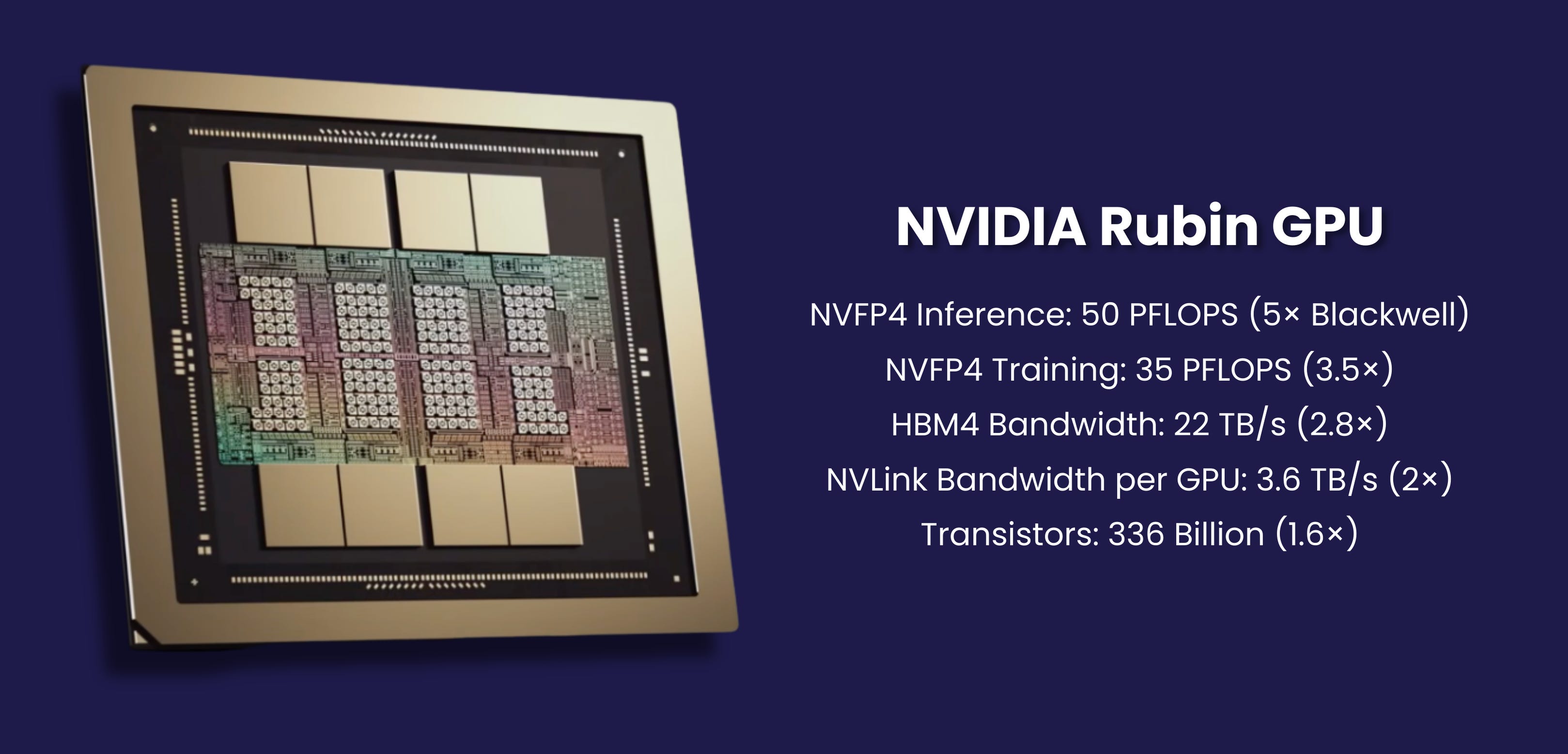
Rubin GPUs deliver ~5× inference performance over Blackwell
With only ~1.6× more transistors
That gain didn’t come from a node shrink.
It came from breaking another, more sacred rule.
“Never redesign the whole system at once.”
NVIDIA ignored it. In the age of AI the “safe choice” is now the risky option.
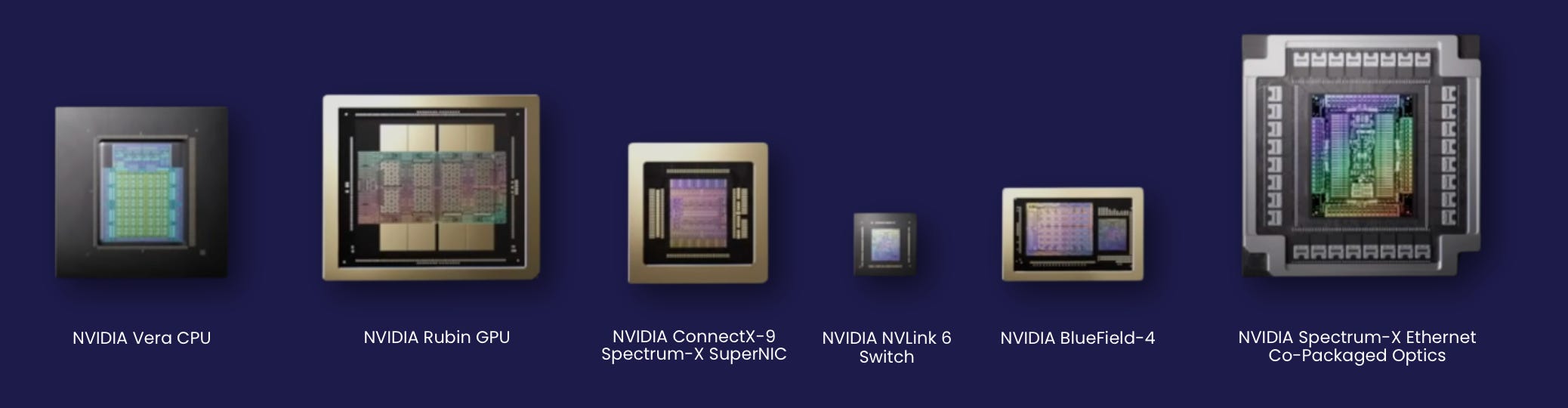
The Six Redesigned Chips
They rebuilt the AI factory as a single machine — in one synchronized generation. Rubin is not “a GPU launch.” It’s a six‑chip platform:
Vera CPU
Rubin GPU
NVLink 6 switch
ConnectX‑9 SuperNIC
BlueField‑4 DPU
Spectrum‑6 / Spectrum‑X Ethernet with co‑packaged optics
The Six Chips — What Each One Actually Does (In Plain Terms)
Think of Rubin not as a GPU upgrade, but as a machine where no part is allowed to wait and every chip exists to eliminate a different kind of stall.
1) Rubin GPU — The Thinker
What it does:
The Rubin GPU does the thinking — matrix math, attention, token generation.
What changed:
It’s not built to be “good at all math.” It’s built to be exceptionally good at the math AI actually uses today: low-precision inference and training (NVFP4).
Why that matters:
Modern AI isn’t limited by raw arithmetic. It’s limited by how fast data can be moved in and out of the GPU.
By lowering precision and redesigning the execution engine, Rubin gets far more useful work per transistor and per watt.
Intuition:
Rubin isn’t a faster brain — it’s a brain that wastes less time thinking about irrelevant details.
2) Vera CPU — The Traffic Controller
What it does:
The Vera CPU doesn’t “think.” It coordinates.
It schedules work, manages memory addresses, launches kernels, and ensures GPUs are never idle.
What changed:
Unlike traditional CPUs designed for browsers, databases, and operating systems, Vera is purpose-built to feed accelerators.
Why that matters:
In large AI systems, GPUs don’t stall because they’re slow — they stall because the CPU can’t keep up with orchestration.
Intuition:
If the GPU is the engine, the Vera CPU is the pit crew — invisible when it’s good, catastrophic when it’s not.
3) NVLink 6 — The Internal Nervous System
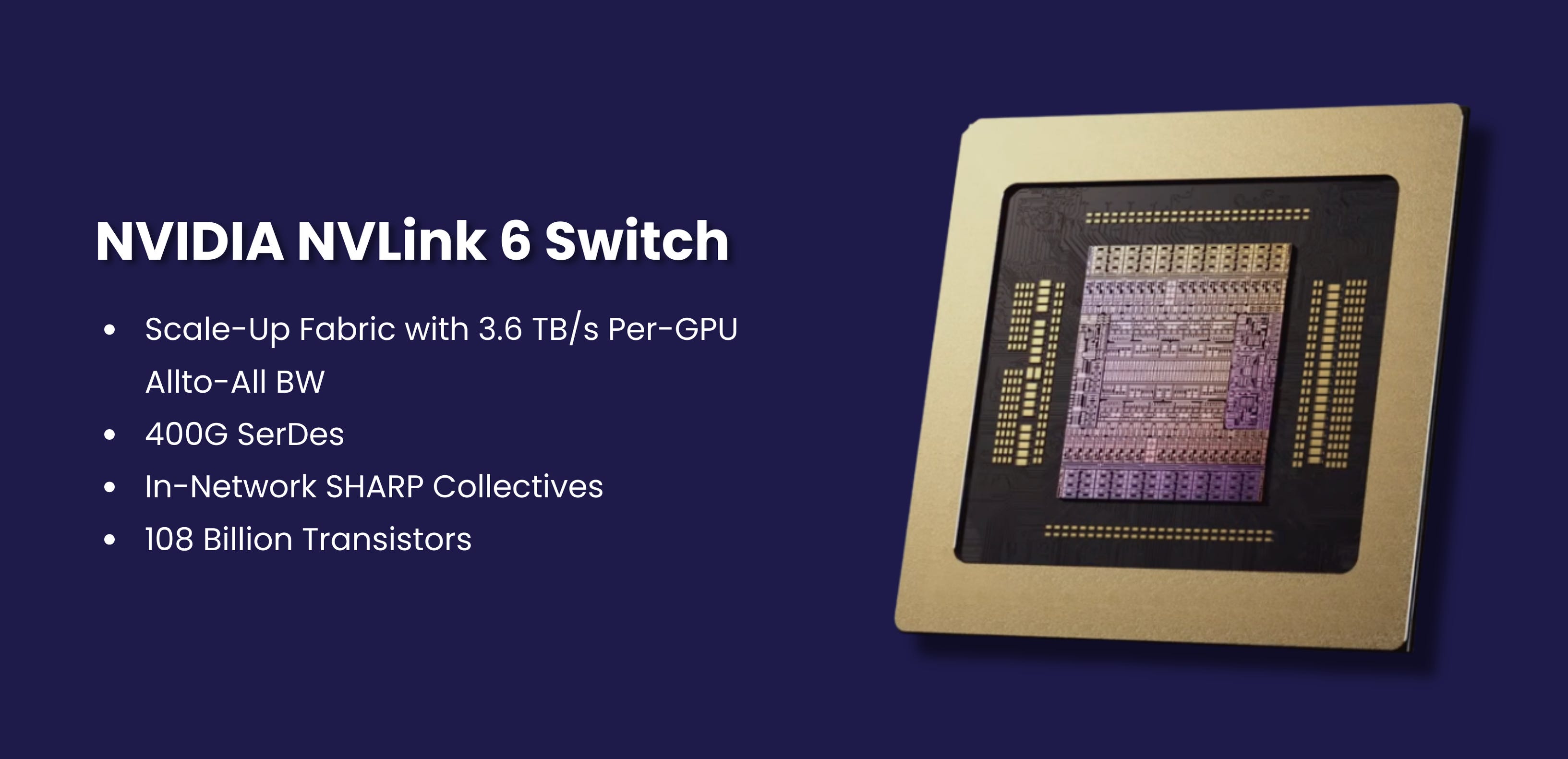
What it does:
NVLink connects GPUs to each other as if they were one device.
What changed:
NVLink 6 is fast enough that dozens of GPUs can share work without constantly stopping to synchronize.
Why that matters:
Large models — especially Mixture-of-Experts — require GPUs to constantly exchange partial results.
If that exchange is slow, everything slows.
Intuition:
NVLink 6 removes the “waiting room” between GPUs. No queues, no traffic jams.
4) ConnectX-9 SuperNIC — The Exit Ramp
What it does:
ConnectX-9 moves data between racks and clusters.
What changed:
It can write data directly into GPU memory (RDMA) without waking up the CPU.
Why that matters:
Cross-rack communication is where most large clusters lose performance. Every unnecessary hop adds latency and idle time.
Intuition:
ConnectX-9 is the highway on-ramp that lets GPUs talk to the outside world without stopping at toll booths.
5) BlueField-4 DPU — The Memory That Lets AI Think Longer
This is the most important chip people misunderstand.
What it does:
BlueField-4 manages context memory — the long-term working memory of AI models.
What changed:
Reasoning and agentic models need to remember a lot: conversation history, tool outputs, intermediate steps.
That memory lives in the KV cache — and it grows fast.
Instead of letting the GPU’s HBM fill up with old context, BlueField-4 provides a dedicated memory tier:
Massive “far memory” for KV cache
GPU-adjacent, low-latency, secure
Why that matters:
HBM should be used for active thinking, not hoarding old memories.
Intuition:
BlueField-4 is the difference between:
a human trying to think while holding every past conversation in their head
and one who can write notes instantly and recall them without effort
This is what makes long-horizon reasoning and agents economically viable.
6) Spectrum-X Ethernet — The Referee
What it does:
Spectrum-X keeps the network predictable under chaos.
What changed:
Traditional Ethernet drops packets when congested — fine for web traffic, disastrous for AI training and inference.
Spectrum-X uses telemetry from the NICs and DPUs to manage congestion before it happens.
Why that matters:
When packets stall, GPUs stall. When GPUs stall, the entire factory loses money.
Intuition:
Spectrum-X doesn’t make the network faster — it makes it reliable when everything is talking at once.
The System-Level Insight (Why All Six Had to Be Built Together)
Each chip removes a different bottleneck:
GPU → compute stall
CPU → orchestration stall
NVLink → synchronization stall
ConnectX → cluster stall
BlueField → memory/context stall
Spectrum → network stall
If you fix only one, another becomes the limit.
Here’s the trap NVIDIA has effectively avoided: once you’re training and serving frontier models at scale, the GPU stops being “the computer” and becomes one stage in a pipeline and pipelines don’t speed up when only one stage gets faster. MoE makes this visible (less compute per token, more expert routing), but it’s not a MoE story; it’s the trajectory of all future AI and robotics workloads: more sparsity, more modularity, more agents, more retrieval, more multimodal streams, more long-horizon state, tighter real‑time loops meaning the scarce resource shifts from raw FLOPs to movement and coordination of state (bandwidth, latency, memory hierarchy, synchronization, determinism). So a 5× faster GPU stapled onto a 2× faster fabric doesn’t produce 5× progress—it produces a machine that waits 3× more efficiently, burning capital and watts to idle. Rubin’s core logic is the only sustainable escape hatch: stop measuring chips and start measuring utilization by co-designing the whole path from compute → memory tiers → scale-up → scale-out → orchestration so the bottleneck can’t simply migrate to “the interface.” That’s what makes it futureproof: it’s not optimized for one model trend, it’s optimized for the invariant of the next decade—workloads will keep changing, but the cost of waiting will keep compounding.
That’s why Rubin works — and why Moore’s Law alone can’t deliver these gains anymore.
IF YOU WANT A VISUAL SUPPLY CHAIN BREAKDOWN CHECK THIS LINK OUT. WE HAVE THE SUPPLY CHAIN + ALL COMPANIES (WITH TICKER IF PUBLIC) ON HERE.
The Supply Chain Breakdown
From silica to a Vera Rubin NVL72 rack — how six “chips” become an AI factory
Before you can buy or build a Vera Rubin NVL72 rack, you have to build something much stranger: a global relay race that starts with silica rock and ends with a liquid‑cooled, rack‑scale supercomputer.
NVIDIA’s own “ground truth” specs are a useful anchor: Vera Rubin NVL72 is a rack system with 72 Rubin GPUs and 36 Vera CPUs, delivering 20.7 TB of HBM4 and 54 TB of LPDDR5X, plus a rack‑scale NVLink domain (260 TB/s) and scale‑out bandwidth (115 TB/s).
Per Rubin GPU, NVIDIA publishes 288 GB HBM4, 22 TB/s memory bandwidth, 3.6 TB/s NVLink, and a key clue: “Total NVIDIA + HBM4 chips: 12.”
That “12 chips” line is the tell: what looks like “one GPU” is actually a dense multi‑chip package where memory and advanced packaging are as important as the compute die itself. And that’s why this supply chain reads like a story.
Below is the story structure we’ll keep repeating for each major component:
Atoms → Ingredients (silica, copper, fluorine chemistry, ultra‑pure gases, ultrapure water)
Blueprints (EDA + IP + verification)
Printing (foundry wafer fabrication)
Grading (wafer test: keep only known‑good die)
Boxing (packaging: substrates, bumps, underfill, 2.5D/3D integration, test)
Turning parts into products (PCBs, connectors, optics, cooling hardware, system integration)
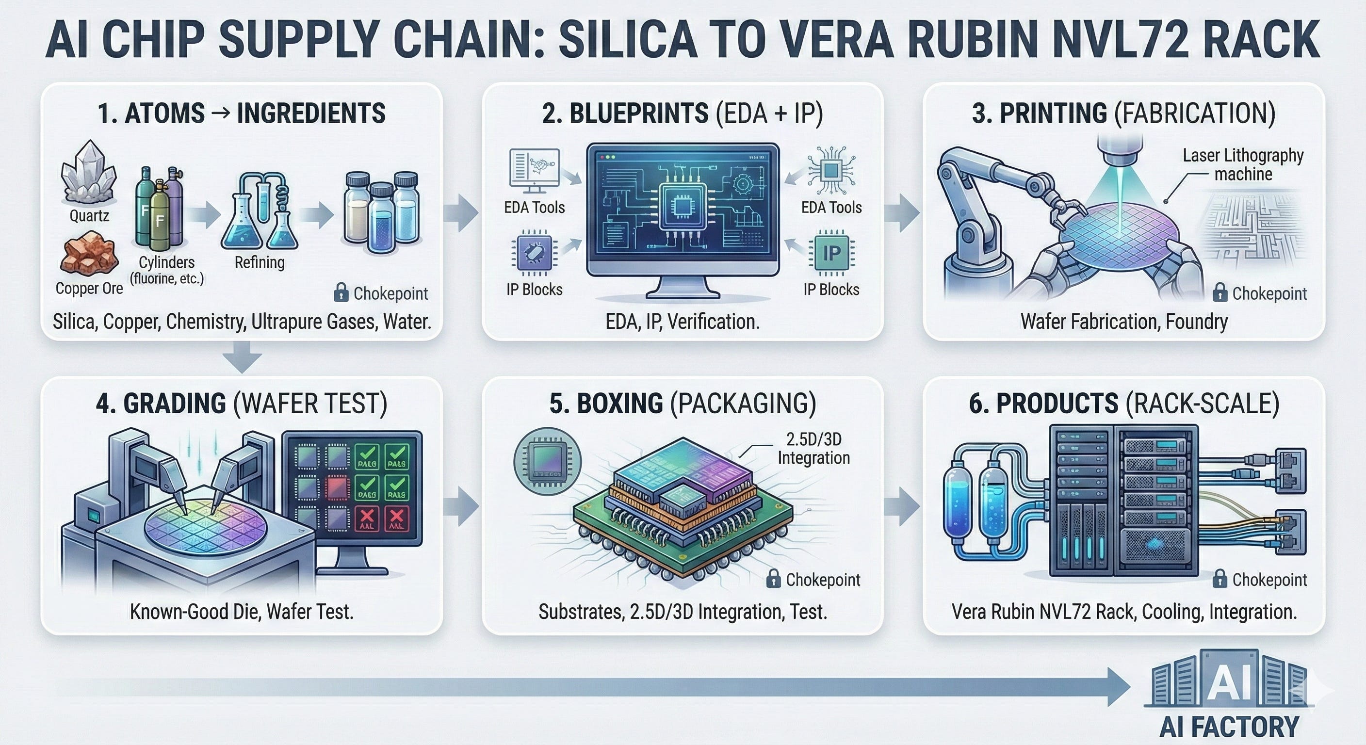
And along the way we’ll call out the industrial “monopolies” / chokepoints investors and operators should care about.
Chapter 0 — The shared foundation: how “sand” becomes chip‑grade reality
0.1 The silica chain: from quartz to 300mm wafers (the “canvas”)
It starts with silica (SiO₂) — but not beach sand. Semiconductor supply chains lean on high‑purity quartz because impurity levels that don’t matter in construction can destroy chip yields.
A simplified chain:
Quartz / silica ore → high‑purity feedstock
Examples: Imerys (EPA: NK), Sibelco (private), The Quartz Corp (private)
Silica + carbon + electricity → metallurgical‑grade silicon (MG‑Si)
Examples: Elkem (OSE: ELK), Ferroglobe (NASDAQ: GSM)
MG‑Si → semiconductor‑grade polysilicon (purified to extreme levels)
Examples: Wacker Chemie (XETRA: WCH), Tokuyama (TSE: 4043)
Polysilicon → 300mm prime wafers (the wafer is the “blank canvas”)
A small club of suppliers matters here. TSMC itself lists a set of major raw wafer suppliers and notes the top group accounts for the vast majority of global raw wafer supply.
Names you’ll see repeatedly: Shin‑Etsu Chemical (TSE: 4063), SUMCO (TSE: 3436), GlobalWafers (TWSE: 6488), Siltronic (XETRA: WAF), SK siltron (subsidiary of SK Inc. (KRX: 034730)), Formosa Sumco Technology (TWSE: 3532).
Why this step must exist: if the wafer (the canvas) has defects, every layer printed later inherits that problem. On modern nodes, a tiny defect can wipe out a large die, and Rubin‑class silicon tends to use large die area and advanced packaging, which multiplies the cost of bad yield.
Output: ultra‑flat, ultra‑pure 300mm wafers ready for foundries and memory fabs.
0.2 The “bloodstream”: ultra‑pure gases, chemicals, and ultrapure water
Chipmaking is not just silicon — it’s chemistry logistics.
Industrial gas majors deliver ultra‑high‑purity (UHP) nitrogen/argon/oxygen/hydrogen and specialty gases:
Linde (NYSE: LIN), Air Liquide (EPA: AI), Air Products (NYSE: APD)
Water becomes ultrapure water (UPW) (fabs consume it constantly):
Veolia (EPA: VIE), Ecolab (NYSE: ECL), Kurita Water Industries (TSE: 6370)
Why it must exist: if gas purity drops or UPW supply hiccups, fabs don’t “slow down” — they often stop, because contamination kills yield.
Output: the continuous consumable stream that makes high‑yield manufacturing possible.
0.3 The stencils: masks, resists, and the “photography” step
You can’t build a chip without repeatedly “printing” patterns onto wafers.
Key roles:
Photomask blanks (ultra‑flat glass with demanding defect specs)
Examples: HOYA (TSE: 7741), AGC (TSE: 5201)
Mask writing / photomasks (reticles)
Examples: TOPPAN (TSE: 7911), Dai Nippon Printing (TSE: 7912), Photronics (NASDAQ: PLAB)
Photoresists + developers
Examples: Tokyo Ohka Kogyo (TOK) (TSE: 4186), Shin‑Etsu (TSE: 4063), DuPont (NYSE: DD), Merck KGaA / EMD Electronics (XETRA: MRK)
Why it must exist: lithography is basically nano‑scale photography — resist is the light‑sensitive film, and masks are the negatives.
Output: wafer layers that can be etched/deposited into transistors and interconnect.
0.4 The machine tools: the factories that build the factories
Even if NVIDIA is the “architect,” toolmakers determine what’s physically manufacturable.
Lithography: ASML (NASDAQ: ASML) is the critical name in EUV. ASML itself states it is the only company that makes EUV lithography technology.
Deposition/etch: Applied Materials (NASDAQ: AMAT), Lam Research (NASDAQ: LRCX), Tokyo Electron (TSE: 8035)
Inspection/metrology: KLA (NASDAQ: KLAC)
A fun (and sobering) fact: EUV is so extreme that ASML describes it as using 13.5 nm wavelength light — almost x‑ray range.
ASML also explains EUV light generation as a tin‑droplet plasma process — a laser hits tiny droplets of tin to create EUV light.
IBM notes these EUV tools are shipped in pieces (think jumbo jets), and contain over 100,000 parts.
Why it must exist: at these nodes, you don’t “buy a machine,” you buy a decade of physics and supply chain integration.
Output: the capability to manufacture leading‑edge logic, advanced DRAM layers, and high‑density interconnect.
0.5 The invisible chokepoint: EDA software (blueprints you can actually build)
Before any wafer exists, Rubin‑class silicon must be designed, verified, and “signed off” with industrial EDA toolchains:
Synopsys (NASDAQ: SNPS)
Cadence (NASDAQ: CDNS)
Siemens EDA (part of Siemens AG, XETRA: SIE)
A major industry shift: Synopsys completed its acquisition of Ansys in July 2025, expanding the “silicon to systems” simulation stack under one roof.
Why it must exist: modern chips are too complex to “eyeball.” EDA is the compiler and the building inspector.
Output: tapeout‑ready design databases that can be turned into masks and then silicon.
The six core Rubin‑platform chips
NVIDIA frames Rubin as six new chips working as one system: Vera CPU, Rubin GPU, NVLink 6 switch, ConnectX‑9, BlueField‑4 DPU, and Spectrum‑6 Ethernet.
We’ll follow each from “atoms → product.”
1) Rubin GPU: the execution engine (and the packaging + HBM supply chain magnet)
What it is (NVIDIA ground truth)
Per Rubin GPU in NVL72, NVIDIA publishes:
288 GB HBM4
22 TB/s memory bandwidth
3.6 TB/s NVLink per GPU
“Total NVIDIA + HBM4 chips: 12”
That last line is why Rubin is a supply‑chain story: you’re not just buying a die — you’re buying a multi‑chip package + stacked memory skyscrapers + the ability to assemble them at yield.
The Rubin GPU manufacturing story
Step 1 — Blueprint (NVIDIA + EDA ecosystem)
NVIDIA (NASDAQ: NVDA) defines the GPU architecture, power/thermal envelope, NVLink behavior, memory interface, and packaging targets.
EDA stack: Synopsys (SNPS), Cadence (CDNS), Siemens (SIE). (These are the design compilers and signoff inspectors.)
Why it matters: design choices determine whether the chip is “just hard” or “physically manufacturable at yield.”
Step 2 — Printing compute silicon (foundry + EUV toolchain)
NVIDIA doesn’t typically publish the exact foundry node for each die on marketing pages. Industry reporting and the broader ecosystem point strongly to TSMC leadership‑node manufacturing for Rubin‑generation silicon — but treat node specifics as “reported,” not NVIDIA‑confirmed unless NVIDIA explicitly states it.
Company cast (the “print shop”):
Foundry: TSMC (NYSE: TSM; TWSE: 2330)
Lithography (EUV monopoly): ASML (NASDAQ: ASML)
Deposition/etch: AMAT, LRCX, TEL
Inspection: KLA
Why it matters: wafer starts on advanced nodes are capacity‑constrained by:
EUV tool availability (ASML is sole supplier)
ramp yield physics
tool install/qualification time
Output: wafers containing Rubin compute die(s).
Step 3 — Grading (wafer test: keep only the A‑students)
Before expensive packaging, wafer probe identifies known‑good die:
Test systems: Advantest (TSE: 6857), Teradyne (NASDAQ: TER)
Probe cards: FormFactor (NASDAQ: FORM)
Why it matters: in advanced packaging, a single bad die can scrap an entire assembled module. So test throughput becomes a “hidden” bottleneck.
Output: known‑good die maps.
Step 4 — HBM4: the memory skyscraper (and the new “base die” trap)
We already have a dedicated piece on this but HBM4 is the “skyscraper next to the GPU.” But the part many models miss is: HBM4 increasingly includes a logic base die (a foundry‑made logic layer), and this base die can be customer‑specific — reducing interchangeability between memory suppliers. Reuters has described the move toward customer‑specific logic dies in next‑gen HBM as a factor that tightens supply flexibility.
HBM4 company cast:
Memory makers (DRAM stacks):
SK hynix (KRX: 000660)
Samsung Electronics (KRX: 005930)
Micron (NASDAQ: MU)
Foundry involvement (base die): frequently TSMC (TSM) and/or Samsung Foundry (005930), depending on supplier approach.
Concrete “base die” breadcrumbs from the suppliers themselves:
SK hynix has announced it plans to adopt TSMC’s logic process for the HBM4 base die.
Samsung has described its HBM4 as using a 4nm logic base die.
Micron has stated it is working with TSMC on HBM4E base logic die development.
Why this step must exist: bandwidth and power constraints push memory closer to compute, and stacking (HBM) is how you get “warehouse‑scale bandwidth” without burning impossible power.
Output: qualified HBM4 stacks ready for integration into the GPU package.
Step 5 — Advanced packaging: where Rubin often becomes supply‑constrained
Rubin‑class GPUs don’t just get “packaged,” they get assembled into a 2.5D integrated module (compute die + multiple HBM stacks) that behaves like a mini‑motherboard inside the package.
Two major chokepoints here:
CoWoS‑class integration capacity
TSMC’s annual report describes CoWoS‑L (an RDL‑based CoWoS variant) and notes that CoWoS‑L entered volume production in 2024.
Substrate ecosystem (ABF + substrate makers)
Ajinomoto Build‑up Film (ABF) is the dielectric “plywood” used in high‑end substrates. Ajinomoto itself has claimed extremely high share (“near 100%”) in ABF for package substrates.
Substrate manufacturers (where ABF turns into dense wiring):
Ibiden (TSE: 4062)
Shinko Electric (TSE: 6967)
Unimicron (TWSE: 3037)
AT&S (VIE: ATS)
(often also Kinsus (TWSE: 3189), Samsung Electro‑Mechanics (KRX: 009150) in the broader ecosystem)
Why it matters: even if you have enough GPU dies and enough HBM stacks, you can still be blocked by:
CoWoS capacity
substrate yield/availability
underfill/encapsulation materials (reliability)
packaging test throughput
Output: a finished Rubin GPU package that can be mounted into server trays.
Why Rubin is “the bottleneck item” in plain English
Rubin’s supply isn’t governed by one factory. It’s governed by the minimum of many constrained pipelines:
EUV/advanced node capacity (ASML + foundry)
HBM4 supply (memory fabs) + logic base die coupling to foundry capacity
CoWoS‑class packaging capacity (TSMC)
ABF/substrate availability (Ajinomoto + substrate makers)
This is why GPU “demand” often shows up first as HBM allocation and advanced packaging capex, not as “more silicon wafers.”
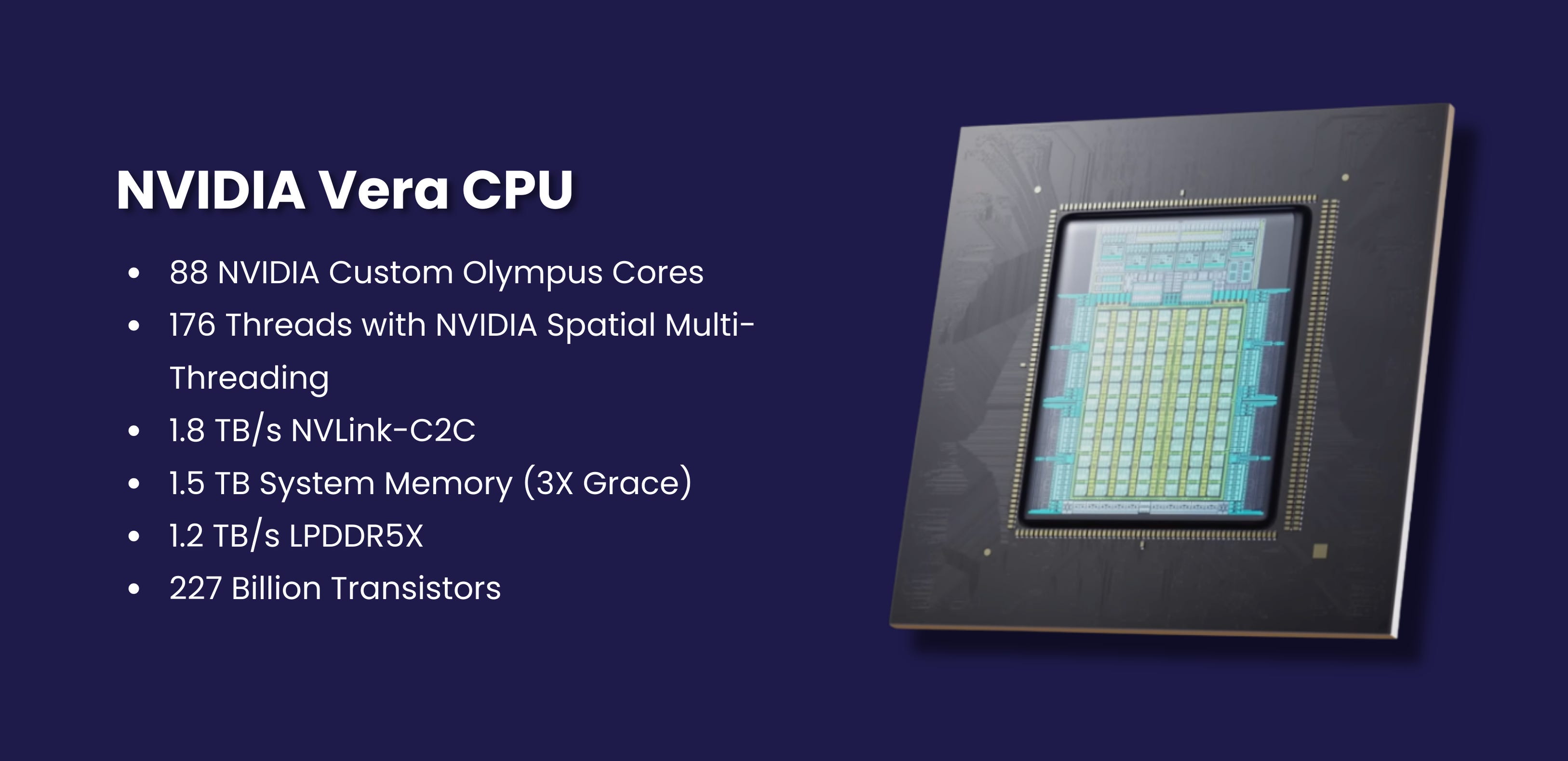
2) Vera CPU: the orchestration engine (and the SOCAMM memory story)
What it is (NVIDIA disclosures)
NVIDIA describes Vera CPU as:
88 custom Olympus CPU cores / 176 threads, Arm‑compatible
1.8 TB/s NVLink‑C2C enabling coherent CPU‑GPU memory
Up to 1.5 TB LPDDR5X via SOCAMM modules, delivering up to 1.2 TB/s memory bandwidth
This matters because Vera isn’t “just a host CPU.” NVIDIA positions it as a high‑bandwidth data movement engine that keeps GPUs utilized at rack scale.
The Vera CPU manufacturing story
Step 1 — Blueprint (NVIDIA + Arm ecosystem + EDA)
Architect + integrator: NVIDIA (NVDA)
ISA/software compatibility: Arm Holdings (NASDAQ: ARM) ecosystem (Vera is Arm‑compatible per NVIDIA’s description).
EDA: SNPS / CDNS / SIE
Why it matters: CPUs are “control‑heavy” silicon; performance is driven by microarchitecture and memory subsystem design. Vera’s defining feature is its memory bandwidth + coherency story.
Output: tapeout‑ready Vera design.
Step 2 — Printing (foundry)
Same global machine tool stack applies:
Foundry: often assumed to be TSMC for this generation, but treat foundry/node specifics as not officially disclosed unless NVIDIA says so on record.
Output: CPU wafers.
Step 3 — Grading (test)
Same test ecosystem: Advantest / Teradyne / FormFactor.
Step 4 — Packaging (large CPU packages are substrate‑hungry)
Vera packages are large, high‑pin‑count, power‑dense devices. They lean heavily on:
ABF film ecosystem (Ajinomoto)
High‑density substrates (Ibiden, Shinko, Unimicron, AT&S)
OSAT/foundry packaging services (often ASE (NYSE: ASX / TWSE: 3711), Amkor (NASDAQ: AMKR), and foundry packaging for leading‑edge designs)
Output: packaged Vera CPUs ready for system integration.
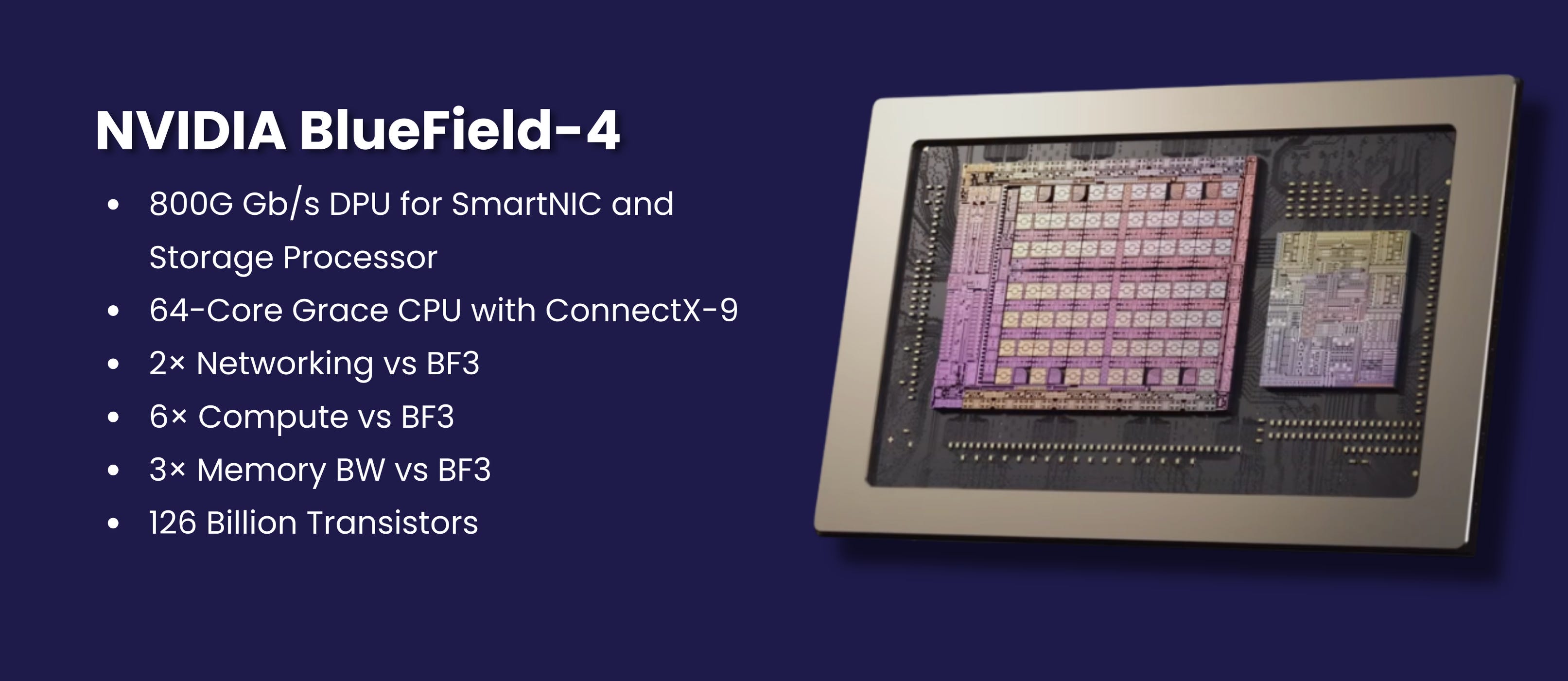
3) BlueField‑4 DPU: the infrastructure processor (the “control plane in silicon”)
What it is (NVIDIA disclosures)
NVIDIA positions BlueField‑4 as part of the six‑chip Rubin platform lineup.
In the NVL72 architecture NVIDIA describes, BlueField‑4 plays a rack‑scale role: secure and accelerate networking, storage, and infrastructure services.
NVIDIA also describes BlueField‑4 in an “Inference Context Memory Storage (ICMS)” context as delivering:
800 Gb/s networking
A 64‑core Grace CPU component
high‑bandwidth LPDDR memory
line‑rate data integrity/encryption features
(For investors/operators: that is NVIDIA explicitly tying a DPU product to both compute and memory requirements — it’s not a tiny sidecar.)
The BlueField‑4 manufacturing story (high‑level)
BlueField looks like a “network card,” but supply chain‑wise it’s closer to: advanced SoC + packaging + board assembly.
Blueprint: NVIDIA (NVDA) + EDA (SNPS/CDNS/SIE)
Printing: leading foundry manufacturing (likely TSMC for Rubin‑generation silicon; treat node per chip as not always publicly itemized)
Grading: Advantest/Teradyne/FormFactor
Packaging: ABF + substrate + OSAT assembly
Board: high‑speed PCB laminates, connectors, VRMs, clocks; then EMS/ODM assembly
Output: BlueField‑4 modules/cards integrated into Rubin compute trays as the “infrastructure processor.”
4) ConnectX‑9 SuperNIC: the endpoint that keeps scale‑out from melting down
What it is (NVIDIA disclosures)
NVIDIA states in its Rubin platform write‑up that each compute tray includes four ConnectX‑9 SuperNIC boards, delivering 1.6 TB/s per Rubin GPU for scale‑out networking.
ConnectX‑9 is listed as one of the six Rubin platform chips.
The ConnectX‑9 manufacturing story
Step 1 — Blueprint (SerDes, PCIe, congestion control logic)
NVIDIA designs the ASIC. High‑speed IO chips are design‑heavy: their “secret sauce” includes SerDes, congestion control behaviors, and offloads — all of which drive link reliability and latency under load.
EDA: SNPS/CDNS/SIE.
Step 2 — Printing (foundry + EUV/DUV stack)
ConnectX‑9 is a high‑performance networking ASIC, likely manufactured on advanced logic nodes.
The upstream chokepoint is the same: lithography tools (ASML), etch/deposition (AMAT/LRCX/TEL), inspection (KLA).
Step 3 — Grading (test)
Test throughput matters because NIC demand scales with GPUs.
Step 4 — Packaging + “board branch”
ConnectX‑9 becomes real supply chain complexity when it turns into a board:
High‑speed PCB materials: low‑loss laminates
Examples: Panasonic (TSE: 6752), Rogers (NYSE: ROG)
PCB fabrication (controlled impedance, multi‑layer):
TTM Technologies (NASDAQ: TTMI), Unimicron (TWSE: 3037), Zhen Ding Tech (TWSE: 4958)
Connectors / cages (OSFP/QSFP ecosystems):
TE Connectivity (NYSE: TEL), Amphenol (NYSE: APH), Molex (private), Samtec (private)
Power delivery (VRMs):
Infineon (XETRA: IFX), Texas Instruments (NASDAQ: TXN), Analog Devices (NASDAQ: ADI), Monolithic Power Systems (NASDAQ: MPWR), Renesas (TSE: 6723), onsemi (NASDAQ: ON)
EMS/ODM assembly:
Hon Hai / Foxconn (TWSE: 2317), Jabil (NYSE: JBL), Flex (NASDAQ: FLEX), Celestica (NYSE: CLS)
Output: SuperNIC boards integrated into compute trays.
5) NVLink 6 Switch ASIC: the “scale‑up spine” inside NVL72
What it is (NVIDIA disclosures)
NVIDIA describes the NVL72 all‑to‑all topology as using 36 NVLink 6 switches, with each switch tray incorporating four NVLink 6 switch chips.
NVLink 6 is part of the six‑chip Rubin platform list.
This is the scale‑up fabric: it is not “Ethernet switching,” it’s the internal GPU‑to‑GPU communication domain that makes rack‑scale training behave like one machine.
The NVLink 6 manufacturing story
NVLink switch silicon is a high‑bandwidth, high‑power ASIC — which means it shares the same underlying constraints as GPUs and NICs:
Blueprint: NVIDIA + EDA
Printing: foundry wafer fab (advanced node)
Grading: wafer test
Packaging: high‑end substrates, large packages, liquid‑cooling integration at tray level
Board: extreme signal integrity (high‑speed PCB materials, connectors)
Output: hot‑swappable NVLink switch trays that create the NVL72 NVLink domain.
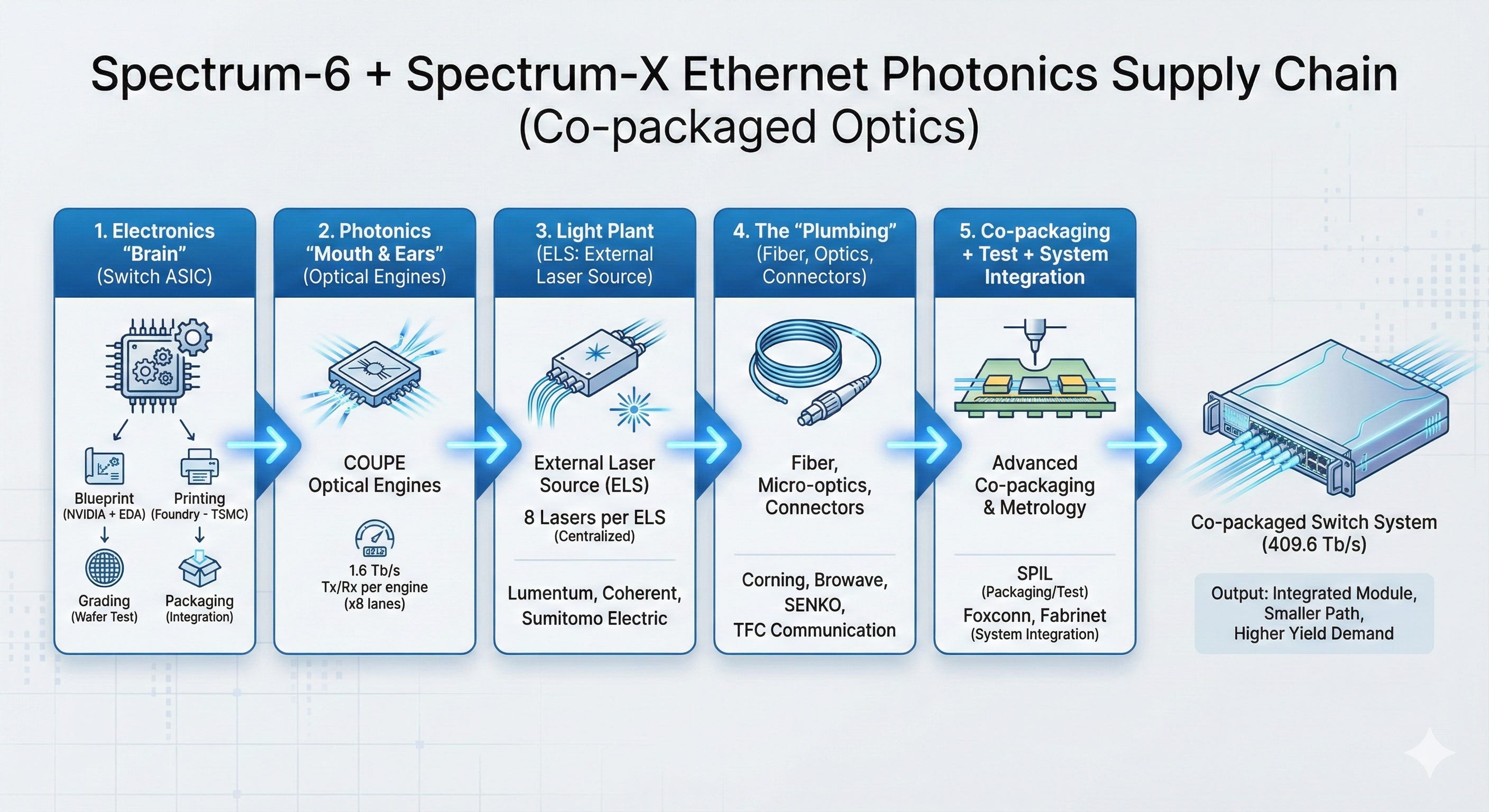
6) Spectrum‑6 + Spectrum‑X Ethernet Photonics (co‑packaged optics): the “future scale‑out” story
This one is worth treating as a different species of supply chain because it blends:
switch ASIC manufacturing (electronics)
silicon photonics (optics on silicon)
laser supply chains (III‑V lasers and optical subassemblies)
fiber/connector precision assembly
advanced co‑packaging / test
What it is (NVIDIA disclosures)
NVIDIA describes Spectrum‑X Ethernet Photonics as co‑packaged optics for Ethernet scale‑out, and says the SN6800 switch delivers 409.6 Tb/s across 512 ports of 800G (or 2,048 ports of 200G) and is coming in 2H 2026.
So you’re not just building a switch — you’re building a switch whose “optical transceivers” are no longer pluggable boxes. They’re integrated into the same module system.
The co‑packaged optics manufacturing story
Step 1 — The electronics “brain” (switch ASIC)
This branch looks like classic chipmaking:
Blueprint: NVIDIA + EDA
Printing: foundry (TSMC is a key ecosystem partner in NVIDIA’s co‑packaged optics collaboration story)
Grading: wafer test
Packaging: advanced package integration
Step 2 — The photonics “mouth and ears” (optical engines)
NVIDIA describes COUPE‑based optical engines in its co‑packaged optics discussion, and gives a concrete throughput framing:
each optical engine supports 1.6 Tb/s transmit and 1.6 Tb/s receive, operating on eight 200 Gb/s lanes in each direction
Step 3 — The light plant (ELS: external laser source)
Instead of embedding lasers everywhere, NVIDIA describes using an External Laser Source (ELS) approach:
each ELS module contains eight lasers
centralizing lasers reduces total lasers (NVIDIA describes reduction by a factor of four)
Key laser ecosystem names NVIDIA calls out in this collaboration context:
Lumentum (NASDAQ: LITE)
Coherent (NYSE: COHR)
Sumitomo Electric (TSE: 5802)
Step 4 — The “plumbing”: fiber, micro‑optics, connectors
NVIDIA’s partner list and narrative ties CPO to fiber/connector specialists, including:
Corning (NYSE: GLW) (fiber ecosystem)
Browave (TPEX: 3163)
SENKO (private)
TFC Communication (noted by NVIDIA as part of the ecosystem)
Step 5 — Co‑packaging + test + system integration (where yield is won or lost)
This is where the supply chain becomes “assembly and metrology heavy.”
NVIDIA explicitly names SPIL for packaging/test roles in the CPO supply chain context, and also points to system assembly players:
Packaging/test: SPIL (Siliconware Precision Industries; part of ASE Technology Holding (NYSE: ASX / TWSE: 3711))
System integration: Hon Hai / Foxconn (TWSE: 2317), Fabrinet (NYSE: FN)
NVIDIA also notes manufacturing details like the use of solder reflow to attach optical engines to substrates in the production flow it describes.
Output: a co‑packaged switch system where electrical paths shrink, and optics become part of the module — but the assembly/test demands rise sharply.
The “supporting cast” that becomes headline constraints
LPDDR5X SOCAMM: why this memory is different (and why it can bottleneck)
LPDDR5X in servers isn’t “phone memory in a rack.” NVIDIA explicitly frames SOCAMM LPDDR5X as a serviceable, power‑efficient memory subsystem enabling up to 1.5 TB per Vera CPU with high bandwidth.
Why SOCAMM is different from standard server DDR:
It’s a module form factor designed around LPDDR behavior (power efficiency, density) and serviceability (replaceable modules rather than soldered packages). NVIDIA specifically highlights serviceability and fault isolation benefits.
The ecosystem is newer and more specialized than commodity RDIMMs.
Who builds SOCAMM modules (and why investors care):
Memory makers: Micron (MU), Samsung (005930), SK hynix (000660) are the prime candidates.
Micron says it is in volume production of SOCAMM, developed with NVIDIA, and positions it as a high‑bandwidth, low‑power, small form‑factor memory module.
Micron also announced SOCAMM2 sampling (up to 192GB) as the ecosystem evolves.
Where SOCAMM bottlenecks show up:
DRAM die supply is necessary but not sufficient — module assembly, PCB/connector tolerances, and qualification become the gating items.
Because SOCAMM is central to Vera’s “coherent memory pool” concept (LPDDR5X + HBM4), shortfalls can degrade system ship volume even if GPUs are available.
SSDs (E1.S NVMe): “boring” until you try to qualify them at NVL72 scale
SSDs are typically more multi‑sourced than GPUs/HBM, but the choke point becomes qualification + form factor + firmware + QoS.
Where SSDs show up in NVIDIA AI racks
NVIDIA DGX documentation describes using E1.S NVMe drives as local storage/cache in rack systems (configurations like multiple E1.S drives in RAID0 are common in this class of platform docs).
Why E1.S matters
E1.S is a standardized “ruler” form factor under SNIA’s SFF work (operators care because hot‑swap serviceability becomes part of uptime).
Two concrete “vendor qualification” signals (GB200 generation, same rack class)
Micron has positioned its 9550 PCIe Gen5 data center SSDs for AI workloads and notes inclusion in NVIDIA ecosystem vendor recommendations for NVL72‑class systems.
Western Digital has stated its DC SN861 E1.S is certified to support NVIDIA GB200 NVL72.
Why this matters for Rubin
Even if SSDs are “available,” the rack builder/operator needs:
firmware compatibility
thermal behavior under rack conditions
latency/QoS behavior
security/telemetry compliance
Output: qualified E1.S SSD SKUs that can ship at rack scale without “mystery latency” incidents.
In the next (paid) section we will talk about the bottlenecks and what companies are set to benefit the most from the increase in demand, and the companies that could be adversely affected due to some of these changes that were previously set to grow
